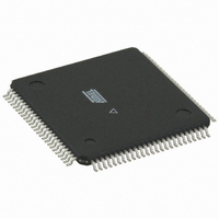
ATMEGA3250P-20AU Atmel, ATMEGA3250P-20AU Datasheet - Page 60

ATMEGA3250P-20AU
Manufacturer Part Number
ATMEGA3250P-20AU
Description
IC MCU AVR 32K FLASH 100-TQFP
Manufacturer
Atmel
Series
AVR® ATmegar
Specifications of ATMEGA3250P-20AU
Core Processor
AVR
Core Size
8-Bit
Speed
20MHz
Connectivity
SPI, UART/USART, USI
Peripherals
Brown-out Detect/Reset, POR, PWM, WDT
Number Of I /o
69
Program Memory Size
32KB (16K x 16)
Program Memory Type
FLASH
Eeprom Size
1K x 8
Ram Size
2K x 8
Voltage - Supply (vcc/vdd)
2.7 V ~ 5.5 V
Data Converters
A/D 8x10b
Oscillator Type
Internal
Operating Temperature
-40°C ~ 85°C
Package / Case
100-TQFP, 100-VQFP
Processor Series
ATMEGA32x
Core
AVR8
Data Bus Width
8 bit
Data Ram Size
2 KB
Interface Type
SPI/UART/USI
Maximum Clock Frequency
20 MHz
Number Of Programmable I/os
69
Number Of Timers
3
Maximum Operating Temperature
+ 85 C
Mounting Style
SMD/SMT
3rd Party Development Tools
EWAVR, EWAVR-BL
Development Tools By Supplier
ATAVRDRAGON, ATSTK500, ATSTK600, ATAVRISP2, ATAVRONEKIT
Minimum Operating Temperature
- 40 C
On-chip Adc
8-ch x 10-bit
For Use With
ATSTK600-TQFP100 - STK600 SOCKET/ADAPTER 100-TQFP770-1007 - ISP 4PORT ATMEL AVR MCU SPI/JTAG770-1005 - ISP 4PORT FOR ATMEL AVR MCU JTAG770-1004 - ISP 4PORT FOR ATMEL AVR MCU SPIATAVRISP2 - PROGRAMMER AVR IN SYSTEMATSTK504 - STARTER KIT AVR EXP MOD 100P LCD
Lead Free Status / RoHS Status
Lead free / RoHS Compliant
Other names
ATMEGA3250P-16AU
ATMEGA3250P-16AU
ATMEGA3250P-16AU
Available stocks
Company
Part Number
Manufacturer
Quantity
Price
Part Number:
ATMEGA3250P-20AU
Manufacturer:
AT
Quantity:
20 000
- Current page: 60 of 364
- Download datasheet (6Mb)
12.3.2
8023F–AVR–07/09
EIMSK – External Interrupt Mask Register
Table 12-1.
• Bit 7 – PCIE3: Pin Change Interrupt Enable 3
When the PCIE3 bit is set (one) and the I-bit in the Status Register (SREG) is set (one), pin
change interrupt 3 is enabled. Any change on any enabled PCINT30:24 pin will cause an inter-
rupt. The corresponding interrupt of Pin Change Interrupt Request is executed from the PCINT3
Interrupt Vector. PCINT30:24 pins are enabled individually by the PCMSK3 Register.
This bit is reserved bit in ATmega325P and should always be written to zero.
• Bit 6 – PCIE2: Pin Change Interrupt Enable 2
When the PCIE2 bit is set (one) and the I-bit in the Status Register (SREG) is set (one), pin
change interrupt 2 is enabled. Any change on any enabled PCINT23:16 pin will cause an inter-
rupt. The corresponding interrupt of Pin Change Interrupt Request is executed from the PCINT2
Interrupt Vector. PCINT23:16 pins are enabled individually by the PCMSK2 Register.
This bit is reserved bit in ATmega325P and should always be written to zero.
• Bit 5 – PCIE1: Pin Change Interrupt Enable 1
When the PCIE1 bit is set (one) and the I-bit in the Status Register (SREG) is set (one), pin
change interrupt 1 is enabled. Any change on any enabled PCINT15:8 pin will cause an inter-
rupt. The corresponding interrupt of Pin Change Interrupt Request is executed from the PCINT1
Interrupt Vector. PCINT15:8 pins are enabled individually by the PCMSK1 Register.
• Bit 4 – PCIE0: Pin Change Interrupt Enable 0
When the PCIE0 bit is set (one) and the I-bit in the Status Register (SREG) is set (one), pin
change interrupt 0 is enabled. Any change on any enabled PCINT7:0 pin will cause an interrupt.
The corresponding interrupt of Pin Change Interrupt Request is executed from the PCINT0 Inter-
rupt Vector. PCINT7:0 pins are enabled individually by the PCMSK0 Register.
• Bit 0 – INT0: External Interrupt Request 0 Enable
When the INT0 bit is set (one) and the I-bit in the Status Register (SREG) is set (one), the exter-
nal pin interrupt is enabled. The Interrupt Sense Control0 bits 1/0 (ISC01 and ISC00) in the
External Interrupt Control Register A (EICRA) define whether the external interrupt is activated
on rising and/or falling edge of the INT0 pin or level sensed. Activity on the pin will cause an
interrupt request even if INT0 is configured as an output. The corresponding interrupt of External
Interrupt Request 0 is executed from the INT0 Interrupt Vector.
Bit
(0xD1)
Read/Write
Initial Value
ISC01
0
0
1
1
Interrupt 0 Sense Control
ISC00
PCIE3
R/W
7
0
0
1
0
1
PCIE2
R/W
Description
The low level of INT0 generates an interrupt request.
Any logical change on INT0 generates an interrupt request.
The falling edge of INT0 generates an interrupt request.
The rising edge of INT0 generates an interrupt request.
6
0
PCIE1
R/W
5
0
PCIE0
R/W
4
0
R
3
–
0
ATmega325P/3250P
R
2
–
0
R
1
–
0
INT0
R/W
0
0
EIMSK
60
Related parts for ATMEGA3250P-20AU
Image
Part Number
Description
Manufacturer
Datasheet
Request
R

Part Number:
Description:
Manufacturer:
Atmel Corporation
Datasheet:

Part Number:
Description:
IC AVR MCU 32K 16MHZ 100TQFP
Manufacturer:
Atmel
Datasheet:

Part Number:
Description:
IC AVR MCU 32K 16MHZ 100TQFP
Manufacturer:
Atmel
Datasheet:

Part Number:
Description:
MCU AVR 32K FLASH 16MHZ 100TQFP
Manufacturer:
Atmel
Datasheet:

Part Number:
Description:
Atmega3250 8-bit Microcontroller With In-system Programmable Flash
Manufacturer:
ATMEL Corporation

Part Number:
Description:
Manufacturer:
Atmel Corporation
Datasheet:

Part Number:
Description:
IC AVR MCU 32K 16MHZ 64-QFN
Manufacturer:
Atmel
Datasheet:

Part Number:
Description:
IC AVR MCU 32K 16MHZ 64TQFP
Manufacturer:
Atmel
Datasheet:

Part Number:
Description:
IC AVR MCU 32K 16MHZ 64TQFP
Manufacturer:
Atmel
Datasheet:

Part Number:
Description:
IC AVR MCU 32K 16MHZ 64-QFN
Manufacturer:
Atmel
Datasheet:

Part Number:
Description:
8-bit Microcontroller with In-System Programmable Flash
Manufacturer:
ATMEL [ATMEL Corporation]
Datasheet:

Part Number:
Description:
MCU AVR 32K FLASH 16MHZ 64TQFP
Manufacturer:
Atmel
Datasheet:

Part Number:
Description:
MCU AVR 32K FLASH 16MHZ 64QFN
Manufacturer:
Atmel
Datasheet:


