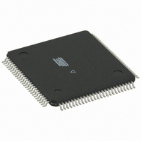
ATMEGA3250P-20AU Atmel, ATMEGA3250P-20AU Datasheet - Page 118

ATMEGA3250P-20AU
Manufacturer Part Number
ATMEGA3250P-20AU
Description
IC MCU AVR 32K FLASH 100-TQFP
Manufacturer
Atmel
Series
AVR® ATmegar
Specifications of ATMEGA3250P-20AU
Core Processor
AVR
Core Size
8-Bit
Speed
20MHz
Connectivity
SPI, UART/USART, USI
Peripherals
Brown-out Detect/Reset, POR, PWM, WDT
Number Of I /o
69
Program Memory Size
32KB (16K x 16)
Program Memory Type
FLASH
Eeprom Size
1K x 8
Ram Size
2K x 8
Voltage - Supply (vcc/vdd)
2.7 V ~ 5.5 V
Data Converters
A/D 8x10b
Oscillator Type
Internal
Operating Temperature
-40°C ~ 85°C
Package / Case
100-TQFP, 100-VQFP
Processor Series
ATMEGA32x
Core
AVR8
Data Bus Width
8 bit
Data Ram Size
2 KB
Interface Type
SPI/UART/USI
Maximum Clock Frequency
20 MHz
Number Of Programmable I/os
69
Number Of Timers
3
Maximum Operating Temperature
+ 85 C
Mounting Style
SMD/SMT
3rd Party Development Tools
EWAVR, EWAVR-BL
Development Tools By Supplier
ATAVRDRAGON, ATSTK500, ATSTK600, ATAVRISP2, ATAVRONEKIT
Minimum Operating Temperature
- 40 C
On-chip Adc
8-ch x 10-bit
For Use With
ATSTK600-TQFP100 - STK600 SOCKET/ADAPTER 100-TQFP770-1007 - ISP 4PORT ATMEL AVR MCU SPI/JTAG770-1005 - ISP 4PORT FOR ATMEL AVR MCU JTAG770-1004 - ISP 4PORT FOR ATMEL AVR MCU SPIATAVRISP2 - PROGRAMMER AVR IN SYSTEMATSTK504 - STARTER KIT AVR EXP MOD 100P LCD
Lead Free Status / RoHS Status
Lead free / RoHS Compliant
Other names
ATMEGA3250P-16AU
ATMEGA3250P-16AU
ATMEGA3250P-16AU
Available stocks
Company
Part Number
Manufacturer
Quantity
Price
Part Number:
ATMEGA3250P-20AU
Manufacturer:
AT
Quantity:
20 000
- Current page: 118 of 364
- Download datasheet (6Mb)
15.8.1
118
ATmega325P/3250P
Compare Output Mode and Waveform Generation
Secondly the COM1x1:0 bits control the OC1x pin output source.
schematic of the logic affected by the COM1x1:0 bit setting. The I/O Registers, I/O bits, and I/O
pins in the figure are shown in bold. Only the parts of the general I/O Port Control Registers
(DDR and PORT) that are affected by the COM1x1:0 bits are shown. When referring to the
OC1x state, the reference is for the internal OC1x Register, not the OC1x pin. If a system reset
occur, the OC1x Register is reset to “0”.
Figure 15-5. Compare Match Output Unit, Schematic
The general I/O port function is overridden by the Output Compare (OC1x) from the Waveform
Generator if either of the COM1x1:0 bits are set. However, the OC1x pin direction (input or out-
put) is still controlled by the Data Direction Register (DDR) for the port pin. The Data Direction
Register bit for the OC1x pin (DDR_OC1x) must be set as output before the OC1x value is visi-
ble on the pin. The port override function is generally independent of the Waveform Generation
mode, but there are some exceptions. Refer to
details.
The design of the Output Compare pin logic allows initialization of the OC1x state before the out-
put is enabled. Note that some COM1x1:0 bit settings are reserved for certain modes of
operation.
The COM1x1:0 bits have no effect on the Input Capture unit.
The Waveform Generator uses the COM1x1:0 bits differently in normal, CTC, and PWM modes.
For all modes, setting the COM1x1:0 = 0 tells the Waveform Generator that no action on the
OC1x Register is to be performed on the next compare match. For compare output actions in the
non-PWM modes refer to
page
page
129.
COMnx1
COMnx0
FOCnx
129, and for phase correct and phase and frequency correct PWM refer to
clk
I/O
See Section “15.11” on page 128.
Waveform
Generator
Table 15-2 on page
D
D
D
PORT
OCnx
DDR
128. For fast PWM mode refer to
Q
Q
Q
Table
15-2,
1
0
Table 15-3
Figure 15-5
and
shows a simplified
Table 15-4
Table 15-3 on
Table 15-4 on
8023F–AVR–07/09
OCnx
Pin
for
Related parts for ATMEGA3250P-20AU
Image
Part Number
Description
Manufacturer
Datasheet
Request
R

Part Number:
Description:
Manufacturer:
Atmel Corporation
Datasheet:

Part Number:
Description:
IC AVR MCU 32K 16MHZ 100TQFP
Manufacturer:
Atmel
Datasheet:

Part Number:
Description:
IC AVR MCU 32K 16MHZ 100TQFP
Manufacturer:
Atmel
Datasheet:

Part Number:
Description:
MCU AVR 32K FLASH 16MHZ 100TQFP
Manufacturer:
Atmel
Datasheet:

Part Number:
Description:
Atmega3250 8-bit Microcontroller With In-system Programmable Flash
Manufacturer:
ATMEL Corporation

Part Number:
Description:
Manufacturer:
Atmel Corporation
Datasheet:

Part Number:
Description:
IC AVR MCU 32K 16MHZ 64-QFN
Manufacturer:
Atmel
Datasheet:

Part Number:
Description:
IC AVR MCU 32K 16MHZ 64TQFP
Manufacturer:
Atmel
Datasheet:

Part Number:
Description:
IC AVR MCU 32K 16MHZ 64TQFP
Manufacturer:
Atmel
Datasheet:

Part Number:
Description:
IC AVR MCU 32K 16MHZ 64-QFN
Manufacturer:
Atmel
Datasheet:

Part Number:
Description:
8-bit Microcontroller with In-System Programmable Flash
Manufacturer:
ATMEL [ATMEL Corporation]
Datasheet:

Part Number:
Description:
MCU AVR 32K FLASH 16MHZ 64TQFP
Manufacturer:
Atmel
Datasheet:

Part Number:
Description:
MCU AVR 32K FLASH 16MHZ 64QFN
Manufacturer:
Atmel
Datasheet:


