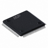
LPC2361FBD100,551 NXP Semiconductors, LPC2361FBD100,551 Datasheet - Page 11

LPC2361FBD100,551
Manufacturer Part Number
LPC2361FBD100,551
Description
IC ARM7 MCU FLASH 64K 100LQFP
Manufacturer
NXP Semiconductors
Series
LPC2300r
Datasheet
1.LPC2361FBD100551.pdf
(57 pages)
Specifications of LPC2361FBD100,551
Program Memory Type
FLASH
Program Memory Size
64KB (64K x 8)
Package / Case
100-LQFP
Core Processor
ARM7
Core Size
16/32-Bit
Speed
72MHz
Connectivity
CAN, I²C, Microwire, SPI, SSI, SSP, UART/USART, USB OTG
Peripherals
Brown-out Detect/Reset, DMA, I²S, POR, PWM, WDT
Number Of I /o
70
Ram Size
34K x 8
Voltage - Supply (vcc/vdd)
3 V ~ 3.6 V
Data Converters
A/D 6x10b; D/A 1x10b
Oscillator Type
Internal
Operating Temperature
-40°C ~ 85°C
Processor Series
LPC23
Core
ARM7TDMI-S
Data Bus Width
16 bit, 32 bit
Data Ram Size
34 KB
Interface Type
CAN/I2S/SPI/SSP/USB
Maximum Clock Frequency
72 MHz
Number Of Programmable I/os
70
Operating Supply Voltage
3.3 V
Maximum Operating Temperature
+ 85 C
Mounting Style
SMD/SMT
3rd Party Development Tools
MDK-ARM, RL-ARM, ULINK2
Minimum Operating Temperature
- 40 C
On-chip Adc
6-ch x 10-bit
On-chip Dac
1-ch x 10-bit
Package
100LQFP
Device Core
ARM7TDMI-S
Family Name
LPC2000
Maximum Speed
72 MHz
Lead Free Status / RoHS Status
Lead free / RoHS Compliant
For Use With
568-4310 - EVAL BOARD LPC2158 W/LCDMCB2360UME - BOARD EVAL MCB2360 + ULINK-MEMCB2360U - BOARD EVAL MCB2360 + ULINK2568-4014 - BOARD EVAL FOR LPC236X ARM568-3999 - BOARD EVAL FOR LPC23 ARM MCU
Eeprom Size
-
Lead Free Status / Rohs Status
Lead free / RoHS Compliant
Other names
568-4525
935286991551
935286991551
Available stocks
Company
Part Number
Manufacturer
Quantity
Price
Company:
Part Number:
LPC2361FBD100,551
Manufacturer:
NXP Semiconductors
Quantity:
10 000
NXP Semiconductors
Table 3.
LPC2361_62_4
Product data sheet
Symbol
P2[7]/RD2/RTS1/
TRACEPKT2
P2[8]/TD2/TXD2/
TRACEPKT3
P2[9]/
USB_CONNECT/
RXD2/EXTIN0
P2[10]/EINT0
P2[11]/EINT1/
I2STX_CLK
P2[12]/EINT2/
I2STX_WS
P2[13]/EINT3/
I2STX_SDA
P3[0] to P3[31]
P3[25]/MAT0[0]/
PWM1[2]
P3[26]/MAT0[1]/
PWM1[3]
P4[0] to P4[31]
Pin description
Pin
66
65
64
53
52
51
50
27
26
[1]
[1]
[1]
[6]
[6]
[6]
[6]
[1]
[1]
…continued
Type
I/O
I
O
O
I/O
O
O
O
I/O
O
I
I
I/O
I
I/O
I
I/O
I/O
I
I/O
I/O
I
I/O
I/O
I/O
O
O
I/O
O
O
I/O
Description
P2[7] — General purpose digital input/output pin.
RD2 — CAN2 receiver input.
RTS1 — Request to Send output for UART1.
TRACEPKT2 — Trace Packet, bit 2.
P2[8] — General purpose digital input/output pin.
TD2 — CAN2 transmitter output.
TXD2 — Transmitter output for UART2.
TRACEPKT3 — Trace Packet, bit 3.
P2[9] — General purpose digital input/output pin.
USB_CONNECT — Signal used to switch an external 1.5 kΩ resistor under
software control. Used with the SoftConnect USB feature.
RXD2 — Receiver input for UART2.
EXTIN0 — External Trigger Input.
P2[10] — General purpose digital input/output pin.
Note: LOW on this pin while RESET is LOW forces on-chip bootloader to take over
control of the part after a reset.
EINT0 — External interrupt 0 input.
P2[11] — General purpose digital input/output pin.
EINT1 — External interrupt 1 input.
I2STX_CLK — Transmit Clock. It is driven by the master and received by the slave.
Corresponds to the signal SCK in the I
P2[12] — General purpose digital input/output pin.
EINT2 — External interrupt 2 input.
I2STX_WS — Transmit Word Select. It is driven by the master and received by the
slave. Corresponds to the signal WS in the I
P2[13] — General purpose digital input/output pin.
EINT3 — External interrupt 3 input.
I2STX_SDA — Transmit data. It is driven by the transmitter and read by the
receiver. Corresponds to the signal SD in the I
Port 3: Port 3 is a 32-bit I/O port with individual direction controls for each bit. The
operation of port 3 pins depends upon the pin function selected via the pin connect
block. Pins 0 through 24, and 27 through 31 of this port are not available.
P3[25] — General purpose digital input/output pin.
MAT0[0] — Match output for Timer 0, channel 0.
PWM1[2] — Pulse Width Modulator 1, output 2.
P3[26] — General purpose digital input/output pin.
MAT0[1] — Match output for Timer 0, channel 1.
PWM1[3] — Pulse Width Modulator 1, output 3.
Port 4: Port 4 is a 32-bit I/O port with individual direction controls for each bit. The
operation of port 4 pins depends upon the pin function selected via the pin connect
block. Pins 0 through 27, 30, and 31 of this port are not available.
Rev. 04 — 4 March 2010
2
S-bus specification.
2
S-bus specification.
2
S-bus specification.
Single-chip 16-bit/32-bit MCU
LPC2361/62
© NXP B.V. 2010. All rights reserved.
11 of 57


