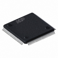
LPC2361FBD100,551 NXP Semiconductors, LPC2361FBD100,551 Datasheet - Page 16

LPC2361FBD100,551
Manufacturer Part Number
LPC2361FBD100,551
Description
IC ARM7 MCU FLASH 64K 100LQFP
Manufacturer
NXP Semiconductors
Series
LPC2300r
Datasheet
1.LPC2361FBD100551.pdf
(57 pages)
Specifications of LPC2361FBD100,551
Program Memory Type
FLASH
Program Memory Size
64KB (64K x 8)
Package / Case
100-LQFP
Core Processor
ARM7
Core Size
16/32-Bit
Speed
72MHz
Connectivity
CAN, I²C, Microwire, SPI, SSI, SSP, UART/USART, USB OTG
Peripherals
Brown-out Detect/Reset, DMA, I²S, POR, PWM, WDT
Number Of I /o
70
Ram Size
34K x 8
Voltage - Supply (vcc/vdd)
3 V ~ 3.6 V
Data Converters
A/D 6x10b; D/A 1x10b
Oscillator Type
Internal
Operating Temperature
-40°C ~ 85°C
Processor Series
LPC23
Core
ARM7TDMI-S
Data Bus Width
16 bit, 32 bit
Data Ram Size
34 KB
Interface Type
CAN/I2S/SPI/SSP/USB
Maximum Clock Frequency
72 MHz
Number Of Programmable I/os
70
Operating Supply Voltage
3.3 V
Maximum Operating Temperature
+ 85 C
Mounting Style
SMD/SMT
3rd Party Development Tools
MDK-ARM, RL-ARM, ULINK2
Minimum Operating Temperature
- 40 C
On-chip Adc
6-ch x 10-bit
On-chip Dac
1-ch x 10-bit
Package
100LQFP
Device Core
ARM7TDMI-S
Family Name
LPC2000
Maximum Speed
72 MHz
Lead Free Status / RoHS Status
Lead free / RoHS Compliant
For Use With
568-4310 - EVAL BOARD LPC2158 W/LCDMCB2360UME - BOARD EVAL MCB2360 + ULINK-MEMCB2360U - BOARD EVAL MCB2360 + ULINK2568-4014 - BOARD EVAL FOR LPC236X ARM568-3999 - BOARD EVAL FOR LPC23 ARM MCU
Eeprom Size
-
Lead Free Status / Rohs Status
Lead free / RoHS Compliant
Other names
568-4525
935286991551
935286991551
Available stocks
Company
Part Number
Manufacturer
Quantity
Price
Company:
Part Number:
LPC2361FBD100,551
Manufacturer:
NXP Semiconductors
Quantity:
10 000
NXP Semiconductors
LPC2361_62_4
Product data sheet
7.5.1 Interrupt sources
7.7.1 Features
7.6 Pin connect block
7.7 General purpose DMA controller
FIQs have the highest priority. If more than one request is assigned to FIQ, the VIC ORs
the requests to produce the FIQ signal to the ARM processor. The fastest possible FIQ
latency is achieved when only one request is classified as FIQ, because then the FIQ
service routine can simply start dealing with that device. But if more than one request is
assigned to the FIQ class, the FIQ service routine can read a word from the VIC that
identifies which FIQ source(s) is (are) requesting an interrupt.
Vectored IRQs, which include all interrupt requests that are not classified as FIQs, have a
programmable interrupt priority. When more than one interrupt is assigned the same
priority and occur simultaneously, the one connected to the lowest numbered VIC channel
will be serviced first.
The VIC ORs the requests from all of the vectored IRQs to produce the IRQ signal to the
ARM processor. The IRQ service routine can start by reading a register from the VIC and
jumping to the address supplied by that register.
Each peripheral device has one interrupt line connected to the VIC but may have several
interrupt flags. Individual interrupt flags may also represent more than one interrupt
source.
Any pin on PORT0 and PORT2 (total of 42 pins) regardless of the selected function, can
be programmed to generate an interrupt on a rising edge, a falling edge, or both. Such
interrupt request coming from PORT0 and/or PORT2 will be combined with the EINT3
interrupt requests.
The pin connect block allows selected pins of the microcontroller to have more than one
function. Configuration registers control the multiplexers to allow connection between the
pin and the on chip peripherals.
Peripherals should be connected to the appropriate pins prior to being activated and prior
to any related interrupt(s) being enabled. Activity of any enabled peripheral function that is
not mapped to a related pin should be considered undefined.
The GPDMA is an AMBA AHB compliant peripheral allowing selected LPC2361/2362
peripherals to have DMA support.
The GPDMA enables peripheral-to-memory, memory-to-peripheral,
peripheral-to-peripheral, and memory-to-memory transactions. Each DMA stream
provides unidirectional serial DMA transfers for a single source and destination. For
example, a bidirectional port requires one stream for transmit and one for receive. The
source and destination areas can each be either a memory region or a peripheral, and
can be accessed through the AHB master.
•
•
Two DMA channels. Each channel can support a unidirectional transfer.
The GPDMA can transfer data between the 8 kB SRAM and peripherals such as the
two SSP, and I
2
S interfaces.
Rev. 04 — 4 March 2010
Single-chip 16-bit/32-bit MCU
LPC2361/62
© NXP B.V. 2010. All rights reserved.
16 of 57


