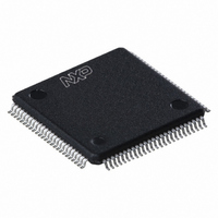
LPC2361FBD100,551 NXP Semiconductors, LPC2361FBD100,551 Datasheet - Page 14

LPC2361FBD100,551
Manufacturer Part Number
LPC2361FBD100,551
Description
IC ARM7 MCU FLASH 64K 100LQFP
Manufacturer
NXP Semiconductors
Series
LPC2300r
Datasheet
1.LPC2361FBD100551.pdf
(57 pages)
Specifications of LPC2361FBD100,551
Program Memory Type
FLASH
Program Memory Size
64KB (64K x 8)
Package / Case
100-LQFP
Core Processor
ARM7
Core Size
16/32-Bit
Speed
72MHz
Connectivity
CAN, I²C, Microwire, SPI, SSI, SSP, UART/USART, USB OTG
Peripherals
Brown-out Detect/Reset, DMA, I²S, POR, PWM, WDT
Number Of I /o
70
Ram Size
34K x 8
Voltage - Supply (vcc/vdd)
3 V ~ 3.6 V
Data Converters
A/D 6x10b; D/A 1x10b
Oscillator Type
Internal
Operating Temperature
-40°C ~ 85°C
Processor Series
LPC23
Core
ARM7TDMI-S
Data Bus Width
16 bit, 32 bit
Data Ram Size
34 KB
Interface Type
CAN/I2S/SPI/SSP/USB
Maximum Clock Frequency
72 MHz
Number Of Programmable I/os
70
Operating Supply Voltage
3.3 V
Maximum Operating Temperature
+ 85 C
Mounting Style
SMD/SMT
3rd Party Development Tools
MDK-ARM, RL-ARM, ULINK2
Minimum Operating Temperature
- 40 C
On-chip Adc
6-ch x 10-bit
On-chip Dac
1-ch x 10-bit
Package
100LQFP
Device Core
ARM7TDMI-S
Family Name
LPC2000
Maximum Speed
72 MHz
Lead Free Status / RoHS Status
Lead free / RoHS Compliant
For Use With
568-4310 - EVAL BOARD LPC2158 W/LCDMCB2360UME - BOARD EVAL MCB2360 + ULINK-MEMCB2360U - BOARD EVAL MCB2360 + ULINK2568-4014 - BOARD EVAL FOR LPC236X ARM568-3999 - BOARD EVAL FOR LPC23 ARM MCU
Eeprom Size
-
Lead Free Status / Rohs Status
Lead free / RoHS Compliant
Other names
568-4525
935286991551
935286991551
Available stocks
Company
Part Number
Manufacturer
Quantity
Price
Company:
Part Number:
LPC2361FBD100,551
Manufacturer:
NXP Semiconductors
Quantity:
10 000
NXP Semiconductors
LPC2361_62_4
Product data sheet
7.2 On-chip flash programming memory
7.3 On-chip SRAM
7.4 Memory map
decode mechanism are much simpler than those of microprogrammed complex
instruction set computers. This simplicity results in a high instruction throughput and
impressive real-time interrupt response from a small and cost-effective processor core.
Pipeline techniques are employed so that all parts of the processing and memory systems
can operate continuously. Typically, while one instruction is being executed, its successor
is being decoded, and a third instruction is being fetched from memory.
The ARM7TDMI-S processor also employs a unique architectural strategy known as
Thumb, which makes it ideally suited to high-volume applications with memory
restrictions, or applications where code density is an issue.
The key idea behind Thumb is that of a super-reduced instruction set. Essentially, the
ARM7TDMI-S processor has two instruction sets:
The Thumb set’s 16-bit instruction length allows it to approach twice the density of
standard ARM code while retaining most of the ARM’s performance advantage over a
traditional 16-bit processor using 16-bit registers. This is possible because Thumb code
operates on the same 32-bit register set as ARM code.
Thumb code is able to provide up to 65 % of the code size of ARM, and 160 % of the
performance of an equivalent ARM processor connected to a 16-bit memory system.
The LPC2361/2362 incorporate a 64 kB and 128 kB flash memory system respectively.
This memory may be used for both code and data storage. Programming of the flash
memory may be accomplished in several ways. It may be programmed In System via the
serial port (UART0). The application program may also erase and/or program the flash
while the application is running, allowing a great degree of flexibility for data storage field
and firmware upgrades.
The flash memory is 128 bits wide and includes pre-fetching and buffering techniques to
allow it to operate at SRAM speeds of 72 MHz.
The LPC2361/2362 include SRAM memory of 8 kB (LPC2361) or 32 kB (LPC2362),
reserved for the ARM processor exclusive use. This RAM may be used for code and/or
data storage and may be accessed as 8 bits, 16 bits, and 32 bits.
A 16 kB SRAM block serving as a buffer for the Ethernet controller (available as general
purpose SRAM for the LPC2361) and an 8 kB SRAM used by the GPDMA controller or
the USB device can be used both for data and code storage. The 2 kB RTC SRAM can be
used for data storage only. The RTC SRAM is battery powered and retains the content in
the absence of the main power supply.
The LPC2361/2362 memory map incorporates several distinct regions as shown in
Figure
•
•
The standard 32-bit ARM set
A 16-bit Thumb set
3.
Rev. 04 — 4 March 2010
Single-chip 16-bit/32-bit MCU
LPC2361/62
© NXP B.V. 2010. All rights reserved.
14 of 57


