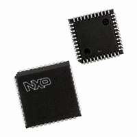
P87C591VFA/00,512 NXP Semiconductors, P87C591VFA/00,512 Datasheet - Page 125

P87C591VFA/00,512
Manufacturer Part Number
P87C591VFA/00,512
Description
IC 80C51 MCU 16K OTP 44-PLCC
Manufacturer
NXP Semiconductors
Series
87Cr
Datasheet
1.P87C591VFA00512.pdf
(160 pages)
Specifications of P87C591VFA/00,512
Core Processor
8051
Core Size
8-Bit
Speed
12MHz
Connectivity
CAN, EBI/EMI, I²C, UART/USART
Peripherals
POR, PWM, WDT
Number Of I /o
32
Program Memory Size
16KB (16K x 8)
Program Memory Type
OTP
Ram Size
512 x 8
Voltage - Supply (vcc/vdd)
4.75 V ~ 5.25 V
Data Converters
A/D 6x10b
Oscillator Type
Internal
Operating Temperature
-40°C ~ 85°C
Package / Case
44-PLCC
Processor Series
P87C5x
Core
80C51
Data Bus Width
8 bit
Data Ram Size
512 B
Interface Type
CAN, I2C, UART
Maximum Clock Frequency
12 MHz
Number Of Programmable I/os
32
Number Of Timers
3
Maximum Operating Temperature
+ 85 C
Mounting Style
SMD/SMT
3rd Party Development Tools
PK51, CA51, A51, ULINK2
Minimum Operating Temperature
- 40 C
On-chip Adc
10 bit, 6 Channel
Lead Free Status / RoHS Status
Lead free / RoHS Compliant
Eeprom Size
-
Lead Free Status / Rohs Status
Details
Other names
568-1256-5
935268182512
P87C591VFAA
935268182512
P87C591VFAA
Available stocks
Company
Part Number
Manufacturer
Quantity
Price
Company:
Part Number:
P87C591VFA/00,512
Manufacturer:
TI
Quantity:
8
Company:
Part Number:
P87C591VFA/00,512
Manufacturer:
NXP Semiconductors
Quantity:
10 000
Philips Semiconductors
20.3
Figure 48 shows the elements of a successive
approximation (SA) ADC. The ADC contains a DAC which
converts of a successive approximation register to a
voltage (VDAC) which is compared to the analog input
voltage (V
successive approximation control logic which controls the
successive approximation register. A conversion is
initiated by setting ADCS in ADCON register. ADCS can
bet set by software only.
The software start mode is selected when control bit
ADCON.5 (ADEX) = 0. A conversion is then started by
setting control bit ADCON.3 (ADCS). The software start
mode is selected when ADCON.5 = 1, and a conversion
may be started by setting ADCON.3.
When a conversion is initiated, the conversion starts at the
beginning of the machine cycle which follows the
instruction that sets ADCS. ADCS is actually implemented
with two flip-flops; a command flip-flop which is affected by
set operations, and a status flag which is accessed during
read operations.
2000 Jul 26
handbook, full pagewidth
Single-chip 8-bit microcontroller with CAN controller
10-Bit Analog-to-Digital Conversion
IN
ADC0
ADC1
ADC2
ADC3
ADC4
ADC5
). The output of the comparator is fed to the
n.c.
n.c.
ADCON
ANALOG INPUT
MULTIPLEXER
0
1
2
Fig.48 Functional diagram of Analog Input Circuitry.
3
4
5
6
7
INTERNAL BUS
10-BIT A/D CONVERTER
0
125
1
The next two machine cycles are used to initiate the
converter. At the end of the first cycle, the ADCS status
flag is set and a value of “1” will be returned if the ADCS
flag is read while the conversion is progress. Sampling of
the analog input commences at the end of the second
cycle.
During the next eight machine cycles, the voltage at the
previously selected pin of port 1 is sampled, and this input
voltage should be stable in order to obtain a useful sample.
In any event, the input voltage slew rate must be less than
10 V/ms in order to prevent an undefined result.
The successive approximation control logic first sets the
most significant bit and clears all other bits in the
successive approximation register (10 0000 0000B). The
output of the DAC (50% full scale) is compared to the input
voltage V
the bit remains set; otherwise it is cleared.
The successive approximation control logic now sets the
next most significant bit (11 0000 0000B or
01 0000 0000B, depending on the previous result), and
VDAC is compared to V
greater than VDAC, then the bit being tested remains set;
2
3
IN
. If the input voltage is greater than VDAC, then
4
5
6
7
IN
again. If the input voltage is
ADCH
MHI050
ANALOG REF.
ANALOG GROUND
Preliminary Specification
P8xC591


