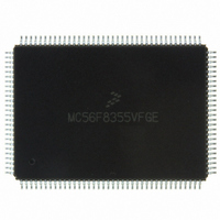
MC56F8355VFGE Freescale Semiconductor, MC56F8355VFGE Datasheet - Page 140

MC56F8355VFGE
Manufacturer Part Number
MC56F8355VFGE
Description
IC DSP 16BIT 60MHZ 128-LQFP
Manufacturer
Freescale Semiconductor
Series
56F8xxxr
Datasheet
1.MC56F8355VFGE.pdf
(172 pages)
Specifications of MC56F8355VFGE
Core Processor
56800
Core Size
16-Bit
Speed
60MHz
Connectivity
CAN, EBI/EMI, SCI, SPI
Peripherals
POR, PWM, Temp Sensor, WDT
Number Of I /o
49
Program Memory Size
264KB (132K x 16)
Program Memory Type
FLASH
Ram Size
10K x 16
Voltage - Supply (vcc/vdd)
2.25 V ~ 3.6 V
Data Converters
A/D 16x12b
Oscillator Type
External
Operating Temperature
-40°C ~ 105°C
Package / Case
128-LQFP
Data Bus Width
16 bit
Processor Series
MC56F83xx
Core
56800E
Numeric And Arithmetic Format
Fixed-Point
Device Million Instructions Per Second
60 MIPs
Maximum Clock Frequency
60 MHz
Number Of Programmable I/os
49
Data Ram Size
20 KB
Maximum Operating Temperature
+ 105 C
Mounting Style
SMD/SMT
Interface Type
SCI, SPI, CAN
Minimum Operating Temperature
- 40 C
For Use With
MC56F8367EVME - EVAL BOARD FOR MC56F83X
Lead Free Status / RoHS Status
Lead free / RoHS Compliant
Eeprom Size
-
Lead Free Status / Rohs Status
Lead free / RoHS Compliant
Available stocks
Company
Part Number
Manufacturer
Quantity
Price
Company:
Part Number:
MC56F8355VFGE
Manufacturer:
Freescale
Quantity:
562
Company:
Part Number:
MC56F8355VFGE
Manufacturer:
Freescale Semiconductor
Quantity:
10 000
Part Number:
MC56F8355VFGE
Manufacturer:
FREESCALE
Quantity:
20 000
10.4 Flash Memory Characteristics
10.5 External Clock Operation Timing
140
•
•
1. There is additional overhead which is part of the programming sequence. See the 56F8300 Peripheral User Manual
2. Specifies page erase time. There are 512 bytes per page in the Data and Boot Flash memories. The Program Flash
1. Parameters listed are guaranteed by design.
2. See
3. The high or low pulse width must be no smaller than 8.0ns or the chip will not function.
4. External clock input rise time is measured from 10% to 90%.
5. External clock input fall time is measured from 90% to 10%.
Characteristic
Program time
Erase time
Mass erase time
Frequency of operation (external clock driver)
Clock Pulse Width
External clock input rise time
External clock input fall time
for details. Program time is per 16-bit word in Flash memory. Two words at a time can be programmed within the Pro-
gram Flash module, as it contains two interleaved memories.
module uses two interleaved Flash memories, increasing the effective page size to 1024 bytes.
Data Valid state, when a signal level has reached V
Data Invalid state, when a signal level is in transition between V
Figure 10-4
Data Invalid State
2
1
Data1 Valid
Table 10-13 External Clock Operation Timing Requirements
Data1
Characteristic
for details on using the recommended connection of an external clock driver.
3
Data Active
5
4
Table 10-12 Flash Timing Parameters
Figure 10-3 Signal States
56F8355 Technical Data, Rev. 17
Data2 Valid
Symbol
T
T
Data2
T
erase
prog
2
me
Symbol
f
t
t
t
osc
PW
rise
fall
OL
Min
100
20
20
or V
Tri-stated
OH
Min
3.0
Data
—
—
0
OL
Typ
—
—
—
and V
Typ
—
—
—
—
OH
Data3 Valid
Data Active
Data3
Max
—
—
—
Max
Freescale Semiconductor
120
10
10
—
1
MHz
Unit
Unit
ms
ms
ns
ns
ns
Preliminary
s


