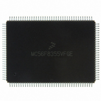
MC56F8355VFGE Freescale Semiconductor, MC56F8355VFGE Datasheet - Page 24

MC56F8355VFGE
Manufacturer Part Number
MC56F8355VFGE
Description
IC DSP 16BIT 60MHZ 128-LQFP
Manufacturer
Freescale Semiconductor
Series
56F8xxxr
Datasheet
1.MC56F8355VFGE.pdf
(172 pages)
Specifications of MC56F8355VFGE
Core Processor
56800
Core Size
16-Bit
Speed
60MHz
Connectivity
CAN, EBI/EMI, SCI, SPI
Peripherals
POR, PWM, Temp Sensor, WDT
Number Of I /o
49
Program Memory Size
264KB (132K x 16)
Program Memory Type
FLASH
Ram Size
10K x 16
Voltage - Supply (vcc/vdd)
2.25 V ~ 3.6 V
Data Converters
A/D 16x12b
Oscillator Type
External
Operating Temperature
-40°C ~ 105°C
Package / Case
128-LQFP
Data Bus Width
16 bit
Processor Series
MC56F83xx
Core
56800E
Numeric And Arithmetic Format
Fixed-Point
Device Million Instructions Per Second
60 MIPs
Maximum Clock Frequency
60 MHz
Number Of Programmable I/os
49
Data Ram Size
20 KB
Maximum Operating Temperature
+ 105 C
Mounting Style
SMD/SMT
Interface Type
SCI, SPI, CAN
Minimum Operating Temperature
- 40 C
For Use With
MC56F8367EVME - EVAL BOARD FOR MC56F83X
Lead Free Status / RoHS Status
Lead free / RoHS Compliant
Eeprom Size
-
Lead Free Status / Rohs Status
Lead free / RoHS Compliant
Available stocks
Company
Part Number
Manufacturer
Quantity
Price
Company:
Part Number:
MC56F8355VFGE
Manufacturer:
Freescale
Quantity:
562
Company:
Part Number:
MC56F8355VFGE
Manufacturer:
Freescale Semiconductor
Quantity:
10 000
Part Number:
MC56F8355VFGE
Manufacturer:
FREESCALE
Quantity:
20 000
24
Signal Name
(GPIOD7)
RXD1
TCK
TMS
TDO
TDI
Table 2-2 Signal and Package Information for the 128-Pin LQFP (Continued)
Pin No.
115
116
117
118
41
Schmitt
Schmitt
Schmitt
Output
Output
Input/
Type
Input
Input
Input
Input
pulled high
pulled high
pulled low
internally
internally
internally
output is
In reset,
disabled
enabled
During
56F8355 Technical Data, Rev. 17
Reset
pullup
State
Input,
Input,
Input,
Input,
Receive Data — SCI1 receive data input
Port D GPIO — This GPIO pin can be individually programmed as
an input or output pin.
After reset, the default state is SCI input.
To deactivate the internal pullup resistor, clear bit 7 in the
GPIOD_PUR register.
Test Clock Input — This input pin provides a gated clock to
synchronize the test logic and shift serial data to the
JTAG/EOnCE port. The pin is connected internally to a pull-down
resistor.
Test Mode Select Input — This input pin is used to sequence the
JTAG TAP controller’s state machine. It is sampled on the rising
edge of TCK and has an on-chip pullup resistor.
To deactivate the internal pullup resistor, set the JTAG bit in the
SIM_PUDR register.
Note:
Test Data Input — This input pin provides a serial input data
stream to the JTAG/EOnCE port. It is sampled on the rising edge
of TCK and has an on-chip pullup resistor.
To deactivate the internal pullup resistor, set the JTAG bit in the
SIM_PUDR register.
Test Data Output — This tri-stateable output pin provides a serial
output data stream from the JTAG/EOnCE port. It is driven in the
shift-IR and shift-DR controller states, and changes on the falling
edge of TCK.
Always tie the TMS pin to V
Signal Description
DD
through a 2.2K resistor.
Freescale Semiconductor
Preliminary


