C8051F504-IM Silicon Laboratories Inc, C8051F504-IM Datasheet - Page 11
C8051F504-IM
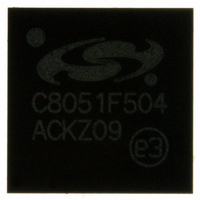
Manufacturer Part Number
C8051F504-IM
Description
IC 8051 MCU 32K FLASH 48-QFN
Manufacturer
Silicon Laboratories Inc
Series
C8051F50xr
Specifications of C8051F504-IM
Program Memory Type
FLASH
Program Memory Size
32KB (32K x 8)
Package / Case
48-QFN
Mfg Application Notes
LIN Bootloader AppNote
Core Processor
8051
Core Size
8-Bit
Speed
50MHz
Connectivity
EBI/EMI, SMBus (2-Wire/I²C), CAN, LIN, SPI, UART/USART
Peripherals
POR, PWM, Temp Sensor, WDT
Number Of I /o
40
Ram Size
4.25K x 8
Voltage - Supply (vcc/vdd)
1.8 V ~ 5.25 V
Data Converters
A/D 32x12b
Oscillator Type
Internal
Operating Temperature
-40°C ~ 125°C
Processor Series
C8051F5x
Core
8051
Data Bus Width
8 bit
Data Ram Size
4.25 KB
Interface Type
I2C/SPI/UART
Maximum Clock Frequency
50 MHz
Number Of Programmable I/os
40
Number Of Timers
4
Maximum Operating Temperature
+ 125 C
Mounting Style
SMD/SMT
3rd Party Development Tools
PK51, CA51, A51, ULINK2
Development Tools By Supplier
C8051F500DK
Minimum Operating Temperature
- 40 C
On-chip Adc
32-ch x 12-bit
Lead Free Status / RoHS Status
Lead free / RoHS Compliant
For Use With
336-1527 - KIT DEV FOR C8051F50X
Eeprom Size
-
Lead Free Status / Rohs Status
Lead free / RoHS Compliant
Other names
336-1519-5
Available stocks
Company
Part Number
Manufacturer
Quantity
Price
Company:

Part Number:
C8051F504-IM
Manufacturer:
Silicon Labs
Quantity:
135


C8051F50x/F51x
List of Tables
Table 2.1. Product Selection Guide ......................................................................... 21
Table 3.1. Pin Definitions for the C8051F50x-F51x ................................................. 22
Table 4.1. QFP-48 Package Dimensions ................................................................ 30
Table 4.2. QFP-48 Landing Diagram Dimensions ................................................... 31
Table 4.3. QFN-48 Package Dimensions ................................................................ 32
Table 4.4. QFN-48 Landing Diagram Dimensions ................................................... 33
Table 4.5. QFN-40 Package Dimensions ................................................................ 34
Table 4.6. QFN-40 Landing Diagram Dimensions ................................................... 35
Table 4.7. QFP-32 Package Dimensions ................................................................ 36
Table 4.8. QFP-32 Landing Diagram Dimensions ................................................... 37
Table 4.9. QFN-32 Package Dimensions ................................................................ 38
Table 4.10. QFN-32 Landing Diagram Dimensions ................................................. 39
Table 5.1. Absolute Maximum Ratings .................................................................... 40
Table 5.2. Global Electrical Characteristics ............................................................. 41
Table 5.3. Port I/O DC Electrical Characteristics ..................................................... 45
Table 5.4. Reset Electrical Characteristics .............................................................. 46
Table 5.5. Flash Electrical Characteristics .............................................................. 46
Table 5.6. Internal High-Frequency Oscillator Electrical Characteristics ................. 47
Table 5.7. Clock Multiplier Electrical Specifications ................................................ 48
Table 5.8. Voltage Regulator Electrical Characteristics .......................................... 48
Table 5.9. ADC0 Electrical Characteristics .............................................................. 49
Table 5.10. Temperature Sensor Electrical Characteristics .................................... 50
Table 5.11. Voltage Reference Electrical Characteristics ....................................... 50
Table 5.12. Comparator 0 and Comparator 1 Electrical Characteristics ................. 51
Table 11.1. CIP-51 Instruction Set Summary (Prefetch-Enabled) ........................... 89
Table 13.1. Special Function Register (SFR) Memory Map for
Pages 0x0 and 0xF ............................................................................. 111
Table 13.2. Special Function Register (SFR) Memory Map for Page 0xC ............ 112
Table 13.3. Special Function Registers ................................................................. 113
Table 14.1. Interrupt Summary .............................................................................. 119
Table 15.1. Flash Security Summary .................................................................... 132
Table 18.1. EMIF Pinout (C8051F500/1/4/5) ......................................................... 149
Table 18.2. EMIF Pinout (C8051F508/9-F510/1) .................................................. 150
Table 18.3. AC Parameters for External Memory Interface ................................... 164
Table 20.1. Port I/O Assignment for Analog Functions ......................................... 179
Table 20.2. Port I/O Assignment for Digital Functions ........................................... 179
Table 20.3. Port I/O Assignment for External Digital Event Capture Functions .... 180
Table 21.1. Baud Rate Calculation Variable Ranges ............................................ 202
Table 21.2. Manual Baud Rate Parameters Examples ......................................... 204
Rev. 1.2
11
Related parts for C8051F504-IM
Image
Part Number
Description
Manufacturer
Datasheet
Request
R

Part Number:
Description:
SMD/C°/SINGLE-ENDED OUTPUT SILICON OSCILLATOR
Manufacturer:
Silicon Laboratories Inc
Part Number:
Description:
Manufacturer:
Silicon Laboratories Inc
Datasheet:
Part Number:
Description:
N/A N/A/SI4010 AES KEYFOB DEMO WITH LCD RX
Manufacturer:
Silicon Laboratories Inc
Datasheet:
Part Number:
Description:
N/A N/A/SI4010 SIMPLIFIED KEY FOB DEMO WITH LED RX
Manufacturer:
Silicon Laboratories Inc
Datasheet:
Part Number:
Description:
N/A/-40 TO 85 OC/EZLINK MODULE; F930/4432 HIGH BAND (REV E/B1)
Manufacturer:
Silicon Laboratories Inc
Part Number:
Description:
EZLink Module; F930/4432 Low Band (rev e/B1)
Manufacturer:
Silicon Laboratories Inc
Part Number:
Description:
I°/4460 10 DBM RADIO TEST CARD 434 MHZ
Manufacturer:
Silicon Laboratories Inc
Part Number:
Description:
I°/4461 14 DBM RADIO TEST CARD 868 MHZ
Manufacturer:
Silicon Laboratories Inc
Part Number:
Description:
I°/4463 20 DBM RFSWITCH RADIO TEST CARD 460 MHZ
Manufacturer:
Silicon Laboratories Inc
Part Number:
Description:
I°/4463 20 DBM RADIO TEST CARD 868 MHZ
Manufacturer:
Silicon Laboratories Inc
Part Number:
Description:
I°/4463 27 DBM RADIO TEST CARD 868 MHZ
Manufacturer:
Silicon Laboratories Inc
Part Number:
Description:
I°/4463 SKYWORKS 30 DBM RADIO TEST CARD 915 MHZ
Manufacturer:
Silicon Laboratories Inc
Part Number:
Description:
N/A N/A/-40 TO 85 OC/4463 RFMD 30 DBM RADIO TEST CARD 915 MHZ
Manufacturer:
Silicon Laboratories Inc
Part Number:
Description:
I°/4463 20 DBM RADIO TEST CARD 169 MHZ
Manufacturer:
Silicon Laboratories Inc