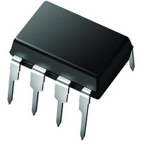
PIC12LC671-04/P Microchip Technology, PIC12LC671-04/P Datasheet - Page 31

PIC12LC671-04/P
Manufacturer Part Number
PIC12LC671-04/P
Description
IC MCU OTP 1KX14 LV A/D 8DIP
Manufacturer
Microchip Technology
Series
PIC® 12Cr
Specifications of PIC12LC671-04/P
Core Processor
PIC
Core Size
8-Bit
Speed
4MHz
Peripherals
POR, WDT
Number Of I /o
5
Program Memory Size
1.75KB (1K x 14)
Program Memory Type
OTP
Ram Size
128 x 8
Voltage - Supply (vcc/vdd)
2.5 V ~ 5.5 V
Data Converters
A/D 4x8b
Oscillator Type
Internal
Operating Temperature
0°C ~ 70°C
Package / Case
8-DIP (0.300", 7.62mm)
Processor Series
PIC12LC
Core
PIC
Data Bus Width
8 bit
Data Ram Size
128 B
Maximum Clock Frequency
4 MHz
Number Of Programmable I/os
5
Number Of Timers
8
Operating Supply Voltage
2.5 V to 5.5 V
Maximum Operating Temperature
+ 70 C
Mounting Style
Through Hole
3rd Party Development Tools
52715-96, 52716-328, 52717-734
Development Tools By Supplier
ICE2000
Minimum Operating Temperature
0 C
On-chip Adc
8
Data Rom Size
128 B
Height
3.3 mm
Length
9.27 mm
Supply Voltage (max)
5.5 V
Supply Voltage (min)
2.5 V
Width
6.35 mm
For Use With
309-1051 - ADAPTER 8-DIP BD W/2 SO PLUGS
Lead Free Status / RoHS Status
Lead free / RoHS Compliant
Eeprom Size
-
Connectivity
-
Lead Free Status / Rohs Status
Details
TABLE 5-1:
5.4
5.4.1
Any instruction which writes, operates internally as a
read followed by a write operation. The BCF and BSF
instructions, for example, read the register into the
CPU, execute the bit operation and write the result back
to the register. Caution must be used when these
instructions are applied to a port with both inputs and
outputs defined. For example, a BSF operation on bit5
of GPIO will cause all eight bits of GPIO to be read into
the CPU. Then the BSF operation takes place on bit5
and GPIO is written to the output latches. If another bit
of GPIO is used as a bi-directional I/O pin (i.e., bit0) and
it is defined as an input at this time, the input signal
present on the pin itself would be read into the CPU and
rewritten to the data latch of this particular pin, overwrit-
ing the previous content. As long as the pin stays in the
input mode, no problem occurs. However, if bit0 is
switched to an output, the content of the data latch may
now be unknown.
Reading the port register reads the values of the port
pins. Writing to the port register writes the value to the
port latch. When using read-modify-write instructions
(i.e., BCF, BSF, etc.) on a port, the value of the port
pins is read, the desired operation is done to this value,
and this value is then written to the port latch.
Address
85h
81h
03h
05h
Legend: Shaded cells not used by Port Registers, read as ‘0’, — = unimplemented, read as '0', x = unknown, u = unchanged,
Note 1: The IRP and RP1 bits are reserved on the PIC12C67X; always maintain these bits clear.
1999 Microchip Technology Inc.
2: The SCL and SDA bits are unimplemented on the PIC12C671 and PIC12C672.
I/O Programming Considerations
BI-DIRECTIONAL I/O PORTS
q = see tables in Section 9.4 for possible values.
TRIS
OPTION
STATUS
GPIO
Name
SUMMARY OF PORT REGISTERS
GPPU
SCL
IRP
Bit 7
—
(1)
(2)
INTEDG
SDA
RP1
Bit 6
—
(2)
(1)
GPIO Data Direction Register
T0CS
Bit 5
RP0
GP5
T0SE
Bit 4
GP4
TO
Bit 3
PSA
GP3
PD
Example 5-1 shows the effect of two sequential read-
modify-write instructions on an I/O port.
EXAMPLE 5-1:
;Initial GPIO Settings
; GPIO<5:3> Inputs
; GPIO<2:0> Outputs
;
;
;
;
;Note that the user may have expected the pin
;values to be --00 pppp. The 2nd BCF caused
;GP5 to be latched as the pin value (High).
A pin actively outputting a Low or High should not be
driven from external devices at the same time in order
to change the level on this pin (“wired-or”, “wired-and”).
The resulting high output currents may damage the
chip.
BCF
BCF
MOVLW 007h
TRIS
Bit 2
GP2
PS2
Z
GPIO, 5
GPIO, 4
GPIO
Bit 1
GP1
PS1
DC
Bit 0
PS0
GP0
READ-MODIFY-WRITE
INSTRUCTIONS ON AN
I/O PORT
C
;--01 -ppp
;--10 -ppp
;--10 -ppp
;
GPIO latch
----------
PIC12C67X
--11 1111
1111 1111
0001 1xxx
11xx xxxx
Power-on
Value on
Reset
DS30561B-page 31
--11 pppp
--11 pppp
--10 pppp
----------
GPIO pins
--11 1111
1111 1111
000q quuu
11uu uuuu
Value on
all other
Resets


