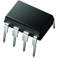
PIC12LC671-04/P Microchip Technology, PIC12LC671-04/P Datasheet - Page 89

PIC12LC671-04/P
Manufacturer Part Number
PIC12LC671-04/P
Description
IC MCU OTP 1KX14 LV A/D 8DIP
Manufacturer
Microchip Technology
Series
PIC® 12Cr
Specifications of PIC12LC671-04/P
Core Processor
PIC
Core Size
8-Bit
Speed
4MHz
Peripherals
POR, WDT
Number Of I /o
5
Program Memory Size
1.75KB (1K x 14)
Program Memory Type
OTP
Ram Size
128 x 8
Voltage - Supply (vcc/vdd)
2.5 V ~ 5.5 V
Data Converters
A/D 4x8b
Oscillator Type
Internal
Operating Temperature
0°C ~ 70°C
Package / Case
8-DIP (0.300", 7.62mm)
Processor Series
PIC12LC
Core
PIC
Data Bus Width
8 bit
Data Ram Size
128 B
Maximum Clock Frequency
4 MHz
Number Of Programmable I/os
5
Number Of Timers
8
Operating Supply Voltage
2.5 V to 5.5 V
Maximum Operating Temperature
+ 70 C
Mounting Style
Through Hole
3rd Party Development Tools
52715-96, 52716-328, 52717-734
Development Tools By Supplier
ICE2000
Minimum Operating Temperature
0 C
On-chip Adc
8
Data Rom Size
128 B
Height
3.3 mm
Length
9.27 mm
Supply Voltage (max)
5.5 V
Supply Voltage (min)
2.5 V
Width
6.35 mm
For Use With
309-1051 - ADAPTER 8-DIP BD W/2 SO PLUGS
Lead Free Status / RoHS Status
Lead free / RoHS Compliant
Eeprom Size
-
Connectivity
-
Lead Free Status / Rohs Status
Details
12.0
Absolute Maximum Ratings †
Ambient temperature under bias...............................................................................................................–40° to +125°C
Storage temperature ............................................................................................................................. –65°C to +150°C
Voltage on any pin with respect to V
Voltage on V
Voltage on MCLR with respect to V
Total power dissipation (Note 1)...........................................................................................................................700 mW
Maximum current out of V
Maximum current into V
Input clamp current, I
Output clamp current, I
Maximum output current sunk by any I/O pin..........................................................................................................25 mA
Maximum output current sourced by any I/O pin ....................................................................................................25 mA
Maximum current sunk by GPIO pins combined ...................................................................................................100 mA
Maximum current sourced by GPIO pins combined..............................................................................................100 mA
† NOTICE: Stresses above those listed under “Absolute Maximum Ratings” may cause permanent damage to the
device. This is a stress rating only and functional operation of the device at those or any other conditions above those
indicated in the operation listings of this specification is not implied. Exposure to maximum rating conditions for
extended periods may affect device reliability.
Note 1: Power dissipation is calculated as follows: Pdis = V
1999 Microchip Technology Inc.
ELECTRICAL SPECIFICATIONS FOR PIC12C67X
DD
with respect to V
IK
OK
(V
DD
SS
I
(V
< 0 or V
pin ..............................................................................................................................150 mA
O
pin ...........................................................................................................................200 mA
< 0 or V
SS
SS
I
SS
> V
................................................................................................................ 0 to +7.0V
(Note 2)..................................................................................................0 to +14V
O
(except V
DD
> V
)
DD
)
DD
and MCLR)................................................... –0.3V to (V
DD
x {I
DD
-
I
OH
} +
{(V
DD
PIC12C67X
- V
OH
) x I
OH
DS30561B-page 89
} + (V
DD
O
+ 0.3V)
l x I
20 mA
20 mA
OL
).


