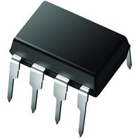
PIC12LC671-04/P Microchip Technology, PIC12LC671-04/P Datasheet - Page 47

PIC12LC671-04/P
Manufacturer Part Number
PIC12LC671-04/P
Description
IC MCU OTP 1KX14 LV A/D 8DIP
Manufacturer
Microchip Technology
Series
PIC® 12Cr
Specifications of PIC12LC671-04/P
Core Processor
PIC
Core Size
8-Bit
Speed
4MHz
Peripherals
POR, WDT
Number Of I /o
5
Program Memory Size
1.75KB (1K x 14)
Program Memory Type
OTP
Ram Size
128 x 8
Voltage - Supply (vcc/vdd)
2.5 V ~ 5.5 V
Data Converters
A/D 4x8b
Oscillator Type
Internal
Operating Temperature
0°C ~ 70°C
Package / Case
8-DIP (0.300", 7.62mm)
Processor Series
PIC12LC
Core
PIC
Data Bus Width
8 bit
Data Ram Size
128 B
Maximum Clock Frequency
4 MHz
Number Of Programmable I/os
5
Number Of Timers
8
Operating Supply Voltage
2.5 V to 5.5 V
Maximum Operating Temperature
+ 70 C
Mounting Style
Through Hole
3rd Party Development Tools
52715-96, 52716-328, 52717-734
Development Tools By Supplier
ICE2000
Minimum Operating Temperature
0 C
On-chip Adc
8
Data Rom Size
128 B
Height
3.3 mm
Length
9.27 mm
Supply Voltage (max)
5.5 V
Supply Voltage (min)
2.5 V
Width
6.35 mm
For Use With
309-1051 - ADAPTER 8-DIP BD W/2 SO PLUGS
Lead Free Status / RoHS Status
Lead free / RoHS Compliant
Eeprom Size
-
Connectivity
-
Lead Free Status / Rohs Status
Details
The ADRES Register contains the result of the A/D
conversion. When the A/D conversion is complete, the
result is loaded into the ADRES register, the GO/DONE
bit (ADCON0<2>) is cleared, and A/D interrupt flag bit
ADIF (PIE1<6>) is set. The block diagrams of the A/D
module are shown in Figure 8-1.
After the A/D module has been configured as desired,
the selected channel must be acquired before the con-
version is started. The analog input channels must
have their corresponding TRIS bits selected as an
input. To determine sample time, see Section 8.1. After
this acquisition time has elapsed, the A/D conversion
can be started. The following steps should be followed
for doing an A/D conversion:
1.
FIGURE 8-1:
1999 Microchip Technology Inc.
Configure the A/D module:
• Configure analog pins / voltage reference /
• Select A/D input channel (ADCON0)
• Select A/D conversion clock (ADCON0)
• Turn on A/D module (ADCON0)
and digital I/O (ADCON1 and TRIS)
Converter
A/D
A/D BLOCK DIAGRAM
(Reference
voltage)
V
REF
(Input voltage)
PCFG<2:0>
V
IN
V
DD
2.
3.
4.
5.
6.
7.
Configure A/D interrupt (if desired):
• Clear ADIF bit
• Set ADIE bit
• Set GIE bit
Wait the required acquisition time.
Start conversion:
• Set GO/DONE bit (ADCON0)
Wait for A/D conversion to complete, by either:
• Polling for the GO/DONE bit to be cleared
OR
• Waiting for the A/D interrupt
Read A/D Result Register (ADRES), clear bit
ADIF if required.
For the next conversion, go to step 1, step 2 or
step 3 as required. The A/D conversion time per
bit is defined as T
required before next acquisition starts.
CHS<1:0>
11
10
01
00
AD
. A minimum wait of 2T
PIC12C67X
DS30561B-page 47
GP2/AN2
GP1/AN1/V
GP0/AN0
GP4/AN3
AD
REF
is


