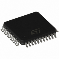
ST72F361J9T6 STMicroelectronics, ST72F361J9T6 Datasheet - Page 168

ST72F361J9T6
Manufacturer Part Number
ST72F361J9T6
Description
IC MCU 8BIT 60K FLASH 44-LQFP
Manufacturer
STMicroelectronics
Series
ST7r
Datasheet
1.ST72F361K6T6.pdf
(225 pages)
Specifications of ST72F361J9T6
Core Processor
ST7
Core Size
8-Bit
Speed
8MHz
Connectivity
LINSCI, SPI
Peripherals
LVD, POR, PWM, WDT
Number Of I /o
32
Program Memory Size
60KB (60K x 8)
Program Memory Type
FLASH
Ram Size
2K x 8
Voltage - Supply (vcc/vdd)
3.8 V ~ 5.5 V
Data Converters
A/D 16x10b
Oscillator Type
External
Operating Temperature
-40°C ~ 85°C
Package / Case
44-LQFP
Processor Series
ST72F3x
Core
ST7
Data Bus Width
8 bit
Data Ram Size
2 KB
Interface Type
LINSCI, SPI
Maximum Clock Frequency
8 MHz
Number Of Programmable I/os
34
Number Of Timers
2
Maximum Operating Temperature
+ 85 C
Mounting Style
SMD/SMT
Development Tools By Supplier
ST72F36X-SK/RAIS, STX-RLINK
Minimum Operating Temperature
- 40 C
On-chip Adc
10 bit, 11 Channel
Lead Free Status / RoHS Status
Lead free / RoHS Compliant
Eeprom Size
-
Lead Free Status / Rohs Status
Details
Available stocks
Company
Part Number
Manufacturer
Quantity
Price
Company:
Part Number:
ST72F361J9T6
Manufacturer:
STMicroelectronics
Quantity:
50
Company:
Part Number:
ST72F361J9T6
Manufacturer:
STMicroelectronics
Quantity:
10 000
- Current page: 168 of 225
- Download datasheet (8Mb)
ST72361
10.9 10-BIT A/D CONVERTER (ADC)
10.9.1 Introduction
The on-chip Analog to Digital Converter (ADC) pe-
ripheral is a 10-bit, successive approximation con-
verter with internal sample and hold circuitry. This
peripheral has up to 16 multiplexed analog input
channels (refer to device pin out description) that
allow the peripheral to convert the analog voltage
levels from up to 16 different sources.
The result of the conversion is stored in a 10-bit
Data Register. The A/D converter is controlled
through a Control/Status Register.
10.9.2 Main Features
■
■
■
■
■
■
The block diagram is shown in
Figure 94. ADC Block Diagram
168/225
10-bit conversion
Up to 16 channels with multiplexed input
Linear successive approximation
Data register (DR) which contains the results
Conversion complete status flag
On/off bit (to reduce consumption)
AIN0
AINx
AIN1
f
CPU
ANALOG
MUX
EOC SPEED ADON SLOW
f
CPU,
Figure
4
ADCDRH
f
CPU
/2
94.
,
f
CPU
ADCDRL
/4
CH3
D9
f
ADC
CH2
D8
10.9.3 Functional Description
10.9.3.1 Digital A/D Conversion Result
The conversion is monotonic, meaning that the re-
sult never decreases if the analog input does not
and never increases if the analog input does not.
If the input voltage (V
(high-level voltage reference) then the conversion
result is FFh in the ADCDRH register and 03h in
the ADCDRL register (without overflow indication).
If the input voltage (V
level voltage reference) then the conversion result
in the ADCDRH and ADCDRL registers is 00 00h.
The A/D converter is linear and the digital result of
the conversion is stored in the ADCDRH and AD-
CDRL registers. The accuracy of the conversion is
described in the Electrical Characteristics Section.
R
for an analog input signal. If the impedance is too
high, this will result in a loss of accuracy due to
leakage and sampling not being completed in the
allotted time.
AIN
CH1
D7
is the maximum recommended impedance
0
CH0
D6
0
D5
ADCCSR
0
D4
0
ANALOG TO DIGITAL
AIN
AIN
D3
) is greater than V
) is lower than V
CONVERTER
0
D2
0
D1
SSA
D0
DDA
(low-
Related parts for ST72F361J9T6
Image
Part Number
Description
Manufacturer
Datasheet
Request
R

Part Number:
Description:
STMicroelectronics [RIPPLE-CARRY BINARY COUNTER/DIVIDERS]
Manufacturer:
STMicroelectronics
Datasheet:

Part Number:
Description:
STMicroelectronics [LIQUID-CRYSTAL DISPLAY DRIVERS]
Manufacturer:
STMicroelectronics
Datasheet:

Part Number:
Description:
BOARD EVAL FOR MEMS SENSORS
Manufacturer:
STMicroelectronics
Datasheet:

Part Number:
Description:
NPN TRANSISTOR POWER MODULE
Manufacturer:
STMicroelectronics
Datasheet:

Part Number:
Description:
TURBOSWITCH ULTRA-FAST HIGH VOLTAGE DIODE
Manufacturer:
STMicroelectronics
Datasheet:

Part Number:
Description:
Manufacturer:
STMicroelectronics
Datasheet:

Part Number:
Description:
DIODE / SCR MODULE
Manufacturer:
STMicroelectronics
Datasheet:

Part Number:
Description:
DIODE / SCR MODULE
Manufacturer:
STMicroelectronics
Datasheet:

Part Number:
Description:
Search -----> STE16N100
Manufacturer:
STMicroelectronics
Datasheet:

Part Number:
Description:
Search ---> STE53NA50
Manufacturer:
STMicroelectronics
Datasheet:

Part Number:
Description:
NPN Transistor Power Module
Manufacturer:
STMicroelectronics
Datasheet:

Part Number:
Description:
DIODE / SCR MODULE
Manufacturer:
STMicroelectronics
Datasheet:


