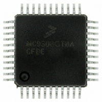
MC9S08GT8ACFBE Freescale Semiconductor, MC9S08GT8ACFBE Datasheet - Page 230

MC9S08GT8ACFBE
Manufacturer Part Number
MC9S08GT8ACFBE
Description
IC MCU 8K FLASH 1K RAM 44-QFP
Manufacturer
Freescale Semiconductor
Series
HCS08r
Datasheet
1.MC9S08GT8ACFBER.pdf
(300 pages)
Specifications of MC9S08GT8ACFBE
Core Processor
HCS08
Core Size
8-Bit
Speed
40MHz
Connectivity
I²C, SCI, SPI
Peripherals
LVD, POR, PWM, WDT
Number Of I /o
36
Program Memory Size
8KB (8K x 8)
Program Memory Type
FLASH
Ram Size
1K x 8
Voltage - Supply (vcc/vdd)
1.8 V ~ 3.6 V
Data Converters
A/D 8x10b
Oscillator Type
Internal
Operating Temperature
-40°C ~ 85°C
Package / Case
44-QFP
Processor Series
S08GT
Core
HCS08
Data Bus Width
8 bit
Data Ram Size
1 KB
Interface Type
I2C/SCI/SPI
Maximum Clock Frequency
40 MHz
Number Of Programmable I/os
36
Operating Supply Voltage
3.6 V
Maximum Operating Temperature
+ 85 C
Mounting Style
SMD/SMT
3rd Party Development Tools
EWS08
Development Tools By Supplier
M68EVB908GB60E, M68DEMO908GB60E
Minimum Operating Temperature
- 40 C
On-chip Adc
8-ch x 10-bit
For Use With
M68DEMO908GB60E - BOARD DEMO MC9S08GB60M68EVB908GB60E - BOARD EVAL FOR MC9S08GB60
Lead Free Status / RoHS Status
Lead free / RoHS Compliant
Eeprom Size
-
Lead Free Status / Rohs Status
Lead free / RoHS Compliant
Available stocks
Company
Part Number
Manufacturer
Quantity
Price
Company:
Part Number:
MC9S08GT8ACFBE
Manufacturer:
FREESCALE
Quantity:
1 600
Company:
Part Number:
MC9S08GT8ACFBE
Manufacturer:
Freescale Semiconductor
Quantity:
10 000
Company:
Part Number:
MC9S08GT8ACFBER
Manufacturer:
Freescale Semiconductor
Quantity:
10 000
- Current page: 230 of 300
- Download datasheet (2Mb)
Analog-to-Digital Converter (S08ATDV3)
14.4
The ATD uses a successive approximation register (SAR) architecture. The ATD contains all the necessary
elements to perform a single analog-to-digital conversion.
A write to the ATDSC register initiates a new conversion. A write to the ATDC register will interrupt the
current conversion but it will not initiate a new conversion. A write to the ATDPE register will also abort
the current conversion but will not initiate a new conversion. If a conversion is already running when a
write to the ATDSC register is made, it will be aborted and a new one will be started.
14.4.1
The ATD has a mode control unit to communicate with the sample and hold (S/H) machine and the SAR
machine when necessary to collect samples and perform conversions. The mode control unit signals the
S/H machine to begin collecting a sample and for the SAR machine to begin receiving a sample. At the
end of the sample period, the S/H machine signals the SAR machine to begin the analog-to-digital
conversion process. The conversion process is terminated when the SAR machine signals the end of
conversion to the mode control unit. For V
to set the sampled signal level within itself without relying on the S/H machine to deliver them.
The mode control unit organizes the conversion, specifies the input sample channel, and moves the digital
output data from the SAR register to the result register. The result register consists of a dual-port register.
The SAR register writes data into the register through one port while the module data bus reads data out
of the register through the other port.
14.4.2
The S/H machine accepts analog signals and stores them as capacitor charge on a storage node located in
the SAR machine. Only one sample can be held at a time so the S/H machine and the SAR machine can
not run concurrently even though they are independent machines.
various resistors and capacitors.
230
Functional Description
Mode Control
Sample and Hold
V
AIN
+
–
Figure 14-10. Resistor and Capacitor Placement
R
AS
MC9S08GT16A/GT8A Data Sheet, Rev. 1
C
AS
REFL
INPUT PIN
INPUT PIN
INPUT PIN
INPUT PIN
and V
R
R
R
R
REFH
AIN1
AIN2
AIN3
AINn
.
.
.
CHANNEL
SELECT 0
CHANNEL
SELECT 1
CHANNEL
SELECT 2
CHANNEL
SELECT n
, the SAR machine uses the reference potentials
Figure 14-10
C
AIN
ATD SAR
ENGINE
shows the placement of the
Freescale Semiconductor
Related parts for MC9S08GT8ACFBE
Image
Part Number
Description
Manufacturer
Datasheet
Request
R
Part Number:
Description:
Manufacturer:
Freescale Semiconductor, Inc
Datasheet:
Part Number:
Description:
Manufacturer:
Freescale Semiconductor, Inc
Datasheet:
Part Number:
Description:
Manufacturer:
Freescale Semiconductor, Inc
Datasheet:
Part Number:
Description:
Manufacturer:
Freescale Semiconductor, Inc
Datasheet:
Part Number:
Description:
Manufacturer:
Freescale Semiconductor, Inc
Datasheet:
Part Number:
Description:
Manufacturer:
Freescale Semiconductor, Inc
Datasheet:
Part Number:
Description:
Manufacturer:
Freescale Semiconductor, Inc
Datasheet:
Part Number:
Description:
Manufacturer:
Freescale Semiconductor, Inc
Datasheet:
Part Number:
Description:
Manufacturer:
Freescale Semiconductor, Inc
Datasheet:
Part Number:
Description:
Manufacturer:
Freescale Semiconductor, Inc
Datasheet:
Part Number:
Description:
Manufacturer:
Freescale Semiconductor, Inc
Datasheet:
Part Number:
Description:
Manufacturer:
Freescale Semiconductor, Inc
Datasheet:
Part Number:
Description:
Manufacturer:
Freescale Semiconductor, Inc
Datasheet:
Part Number:
Description:
Manufacturer:
Freescale Semiconductor, Inc
Datasheet:
Part Number:
Description:
Manufacturer:
Freescale Semiconductor, Inc
Datasheet:


