MC9S08GT8ACFBE Freescale Semiconductor, MC9S08GT8ACFBE Datasheet - Page 273
MC9S08GT8ACFBE
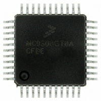
Manufacturer Part Number
MC9S08GT8ACFBE
Description
IC MCU 8K FLASH 1K RAM 44-QFP
Manufacturer
Freescale Semiconductor
Series
HCS08r
Datasheet
1.MC9S08GT8ACFBER.pdf
(300 pages)
Specifications of MC9S08GT8ACFBE
Core Processor
HCS08
Core Size
8-Bit
Speed
40MHz
Connectivity
I²C, SCI, SPI
Peripherals
LVD, POR, PWM, WDT
Number Of I /o
36
Program Memory Size
8KB (8K x 8)
Program Memory Type
FLASH
Ram Size
1K x 8
Voltage - Supply (vcc/vdd)
1.8 V ~ 3.6 V
Data Converters
A/D 8x10b
Oscillator Type
Internal
Operating Temperature
-40°C ~ 85°C
Package / Case
44-QFP
Processor Series
S08GT
Core
HCS08
Data Bus Width
8 bit
Data Ram Size
1 KB
Interface Type
I2C/SCI/SPI
Maximum Clock Frequency
40 MHz
Number Of Programmable I/os
36
Operating Supply Voltage
3.6 V
Maximum Operating Temperature
+ 85 C
Mounting Style
SMD/SMT
3rd Party Development Tools
EWS08
Development Tools By Supplier
M68EVB908GB60E, M68DEMO908GB60E
Minimum Operating Temperature
- 40 C
On-chip Adc
8-ch x 10-bit
For Use With
M68DEMO908GB60E - BOARD DEMO MC9S08GB60M68EVB908GB60E - BOARD EVAL FOR MC9S08GB60
Lead Free Status / RoHS Status
Lead free / RoHS Compliant
Eeprom Size
-
Lead Free Status / Rohs Status
Lead free / RoHS Compliant
Available stocks
Company
Part Number
Manufacturer
Quantity
Price
Company:

Part Number:
MC9S08GT8ACFBE
Manufacturer:
FREESCALE
Quantity:
1 600
Company:
Part Number:
MC9S08GT8ACFBE
Manufacturer:
Freescale Semiconductor
Quantity:
10 000
Company:
Part Number:
MC9S08GT8ACFBER
Manufacturer:
Freescale Semiconductor
Quantity:
10 000


1
2
3
4
5
6
7
8
9
10
11
No.
Freescale Semiconductor
10
11
12
13
14
15
All ACCURACY numbers are based on processor and system being in WAIT state (very little activity and no IO switching) and that
adequate low-pass filtering is present on analog input pins (filter with 0.01 µF to 0.1 µF capacitor between analog input and V
Failure to observe these guidelines may result in system or microcontroller noise causing accuracy errors which will vary based
on board layout and the type and magnitude of the activity.
This is the conversion time for subsequent conversions in continuous convert mode. Actual conversion time for single conversions
or the first conversion in continuous mode is extended by one ATD clock cycle and 2 bus cycles due to starting the conversion and
setting the CCF flag. The total conversion time in Bus Cycles for a conversion is:
charge the input circuitry of the ATD resulting in accuracy error.
Analog input must be between V
scale error (E
The resolution is the ideal step size or 1LSB = (V
Differential non-linearity is the difference between the current code width and the ideal code width (1LSB). The current code width
is the difference in the transition voltages to and from the current code.
Integral non-linearity is the difference between the transition voltage to the current code and the adjusted ideal transition voltage
for the current code. The adjusted ideal transition voltage is (Current Code–1/2)*(1/((V
Zero-scale error is the difference between the transition to the first valid code and the ideal transition to that code. The Ideal
transition voltage to a given code is (Code–1/2)*(1/(V
Full-scale error is the difference between the transition to the last valid code and the ideal transition to that code. The ideal
transition voltage to a given code is (Code–1/2)*(1/(V
Input leakage error is error due to input leakage across the real portion of the impedance of the network driving the analog pin.
Reducing the impedance of the network reduces this error.
Total unadjusted error is the difference between the transition voltage to the current code and the ideal straight-line transfer
function. This measure of error includes inherent quantization error (1/2LSB) and circuit error (differential, integral, zero-scale, and
full-scale) error. The specified value of E
7
8
9
R
AS
is the real portion of the impedance of the network driving the analog input pin. Values greater than this amount may not fully
Ideal resolution (1 LSB)
Differential non-linearity
Integral non-linearity
Zero-scale error
Full-scale error
Input leakage error
Total unadjusted
error
Input resistance
Input capacitance
11
Characteristic
FS
).
SC Bus Cycles = ((PRS+1)*2) * (28+1) + 2
9
8
Table A-9. ATD Timing/Performance Characteristics
10
7
5
6
REFL
1.80V < V
1.80 V < V
2.08V < V
1.80V < V
1.80V < V
1.80V < V
1.80V < V
1.80V < V
and V
T
MC9S08GT16A/GT8A Data Sheet, Rev. 1
assumes zero E
Condition
REFH
DDAD
DDAD
DDAD
DDAD
DDAD
DDAD
DDAD
DDAD
for valid conversion. Values greater than V
REFH
< 2.08V
< 3.6V
< 3.6V
< 3.6V
< 3.6V
< 3.6V
< 3.6V
REFH
REFH
< 3.6V
–V
REFL
–V
–V
IL
(no leakage or zero real source impedance).
REFL
REFL
)/1024
Symbol
CC Bus Cycles = ((PRS+1)*2) * (28)
)).
)).
RES
R
C
DNL
E
E
E
INL
E
AIN
AIN
ZS
FS
TU
IL
2.031
1.758
Min
—
—
—
—
—
—
—
—
1
REFH
(continued)
REFH
+E
+0.05
+0.5
+0.5
+0.4
+0.4
+1.1
Typ
—
—
—
FS
5
)–(V
will convert to $3FF less the full
REFL
Electrical Characteristics
+E
3.516
2.031
Max
+1.0
+1.0
+1.0
+1.0
+2.5
+5
25
7
ZS
))).
Unit
LSB
LSB
LSB
LSB
LSB
LSB
mV
kΩ
pF
REFL
273
).
Related parts for MC9S08GT8ACFBE
Image
Part Number
Description
Manufacturer
Datasheet
Request
R

Part Number:
Description:
Manufacturer:
Freescale Semiconductor, Inc
Datasheet:
Part Number:
Description:
Manufacturer:
Freescale Semiconductor, Inc
Datasheet:
Part Number:
Description:
Manufacturer:
Freescale Semiconductor, Inc
Datasheet:
Part Number:
Description:
Manufacturer:
Freescale Semiconductor, Inc
Datasheet:
Part Number:
Description:
Manufacturer:
Freescale Semiconductor, Inc
Datasheet:
Part Number:
Description:
Manufacturer:
Freescale Semiconductor, Inc
Datasheet:
Part Number:
Description:
Manufacturer:
Freescale Semiconductor, Inc
Datasheet:
Part Number:
Description:
Manufacturer:
Freescale Semiconductor, Inc
Datasheet:
Part Number:
Description:
Manufacturer:
Freescale Semiconductor, Inc
Datasheet:
Part Number:
Description:
Manufacturer:
Freescale Semiconductor, Inc
Datasheet:
Part Number:
Description:
Manufacturer:
Freescale Semiconductor, Inc
Datasheet:
Part Number:
Description:
Manufacturer:
Freescale Semiconductor, Inc
Datasheet:
Part Number:
Description:
Manufacturer:
Freescale Semiconductor, Inc
Datasheet:
Part Number:
Description:
Manufacturer:
Freescale Semiconductor, Inc
Datasheet:
Part Number:
Description:
Manufacturer:
Freescale Semiconductor, Inc
Datasheet: