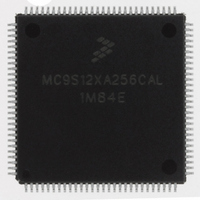
MC9S12XA256CAL Freescale Semiconductor, MC9S12XA256CAL Datasheet - Page 1027

MC9S12XA256CAL
Manufacturer Part Number
MC9S12XA256CAL
Description
IC MCU 256K FLASH 112-LQFP
Manufacturer
Freescale Semiconductor
Series
HCS12r
Specifications of MC9S12XA256CAL
Core Processor
HCS12X
Core Size
16-Bit
Speed
80MHz
Connectivity
EBI/EMI, I²C, IrDA, LIN, SCI, SPI
Peripherals
LVD, POR, PWM, WDT
Number Of I /o
91
Program Memory Size
256KB (256K x 8)
Program Memory Type
FLASH
Eeprom Size
4K x 8
Ram Size
16K x 8
Voltage - Supply (vcc/vdd)
2.35 V ~ 5.5 V
Data Converters
A/D 16x10b
Oscillator Type
External
Operating Temperature
-40°C ~ 85°C
Package / Case
112-LQFP
No. Of I/o's
91
Eeprom Memory Size
4KB
Ram Memory Size
16KB
Cpu Speed
80MHz
No. Of Timers
1
No. Of Pwm Channels
8
Digital Ic Case Style
LQFP
Rohs Compliant
Yes
Processor Series
S12XA
Core
HCS12
Data Bus Width
16 bit
Data Ram Size
16 KB
Interface Type
CAN, I2C, SCI, SPI
Maximum Clock Frequency
40 MHz
Number Of Programmable I/os
91
Number Of Timers
12
Maximum Operating Temperature
+ 85 C
Mounting Style
SMD/SMT
3rd Party Development Tools
EWHCS12
Development Tools By Supplier
EVB9S12XDP512E
Minimum Operating Temperature
- 40 C
On-chip Adc
2 (10 bit, 16 Channel)
Package
112LQFP
Family Name
HCS12
Maximum Speed
40 MHz
Operating Supply Voltage
2.5|5 V
Lead Free Status / RoHS Status
Lead free / RoHS Compliant
Available stocks
Company
Part Number
Manufacturer
Quantity
Price
Company:
Part Number:
MC9S12XA256CAL
Manufacturer:
AD
Quantity:
101
Company:
Part Number:
MC9S12XA256CAL
Manufacturer:
Freescale Semiconductor
Quantity:
10 000
Part Number:
MC9S12XA256CAL
Manufacturer:
FREESCALE
Quantity:
20 000
- Current page: 1027 of 1348
- Download datasheet (8Mb)
Port
AD1
J
1. Each cell represents one register with individual configuration bits
24.0.6
24.0.6.1
This register holds the value driven out to the pin if the pin is used as a general purpose I/O.
Writing to this register has only an effect on the pin if the pin is used as general purpose output.
When reading this address, the buffered state of the pin is returned if the associated data direction
register bit is set to “0”.
If the data direction register bits are set to logic level “1”, the contents of the data register is
returned. This is independent of any other configuration
24.0.6.2
This is a read-only register and always returns the buffered state of the pin
24.0.6.3
This register defines whether the pin is used as an input or an output.
If a peripheral module controls the pin the contents of the data direction register is ignored
(Figure
Data
yes
yes
24-68).
Registers
Data Register
Input Register
Data Direction Register
Direction
Data
yes
yes
Figure 24-68. Illustration of I/O Pin Functionality
Module
Table 24-60. Register Availability per Port
Input
yes
DDR
—
PTI
PT
module enable
data out
output enable
Reduced
Drive
0
1
yes
yes
0
1
0
1
Enable
Pull
yes
yes
(Figure
Polarity
Select
yes
—
24-68).
1
PIN
Wired-OR
Mode
—
—
(Figure
Interrupt
Enable
24-68).
yes
—
Interrupt
Flag
yes
—
Related parts for MC9S12XA256CAL
Image
Part Number
Description
Manufacturer
Datasheet
Request
R
Part Number:
Description:
Manufacturer:
Freescale Semiconductor, Inc
Datasheet:
Part Number:
Description:
Manufacturer:
Freescale Semiconductor, Inc
Datasheet:
Part Number:
Description:
Manufacturer:
Freescale Semiconductor, Inc
Datasheet:
Part Number:
Description:
Manufacturer:
Freescale Semiconductor, Inc
Datasheet:
Part Number:
Description:
Manufacturer:
Freescale Semiconductor, Inc
Datasheet:
Part Number:
Description:
Manufacturer:
Freescale Semiconductor, Inc
Datasheet:
Part Number:
Description:
Manufacturer:
Freescale Semiconductor, Inc
Datasheet:
Part Number:
Description:
Manufacturer:
Freescale Semiconductor, Inc
Datasheet:
Part Number:
Description:
Manufacturer:
Freescale Semiconductor, Inc
Datasheet:
Part Number:
Description:
Manufacturer:
Freescale Semiconductor, Inc
Datasheet:
Part Number:
Description:
Manufacturer:
Freescale Semiconductor, Inc
Datasheet:
Part Number:
Description:
Manufacturer:
Freescale Semiconductor, Inc
Datasheet:
Part Number:
Description:
Manufacturer:
Freescale Semiconductor, Inc
Datasheet:
Part Number:
Description:
Manufacturer:
Freescale Semiconductor, Inc
Datasheet:
Part Number:
Description:
Manufacturer:
Freescale Semiconductor, Inc
Datasheet:


