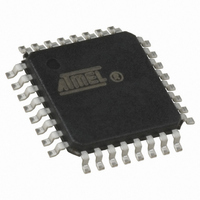
AT90LS2333-4AI Atmel, AT90LS2333-4AI Datasheet - Page 17

AT90LS2333-4AI
Manufacturer Part Number
AT90LS2333-4AI
Description
IC MCU 2K 4MHZ A/D LV IT 32TQFP
Manufacturer
Atmel
Series
AVR® 90LSr
Datasheet
1.AT90LS2333-4AC.pdf
(103 pages)
Specifications of AT90LS2333-4AI
Core Processor
AVR
Core Size
8-Bit
Speed
4MHz
Connectivity
SPI, UART/USART
Peripherals
Brown-out Detect/Reset, POR, PWM, WDT
Number Of I /o
20
Program Memory Size
2KB (1K x 16)
Program Memory Type
FLASH
Eeprom Size
128 x 8
Ram Size
128 x 8
Voltage - Supply (vcc/vdd)
2.7 V ~ 6 V
Data Converters
A/D 6x10b
Oscillator Type
Internal
Operating Temperature
-40°C ~ 85°C
Package / Case
32-TQFP, 32-VQFP
Lead Free Status / RoHS Status
Contains lead / RoHS non-compliant
Status Register - SREG
The AVR status register - SREG - at I/O space location $3F ($5F) is defined as:
•
The global interrupt enable bit must be set (one) for the interrupts to be enabled. The individual interrupt enable control is
then performed in separate control registers. If the global interrupt enable register is cleared (zero), none of the interrupts
are enabled independent of the individual interrupt enable settings. The I-bit is cleared by hardware after an interrupt has
occurred, and is set by the RETI instruction to enable subsequent interrupts.
•
The bit copy instructions BLD (Bit LoaD) and BST (Bit STore) use the T bit as source and destination for the operated bit. A
bit from a register in the register file can be copied into T by the BST instruction, and a bit in T can be copied into a bit in a
register in the register file by the BLD instruction.
•
The half carry flag H indicates a half carry in some arithmetical operations. See the Instruction Set Description for detailed
information.
•
The S-bit is always an exclusive or between the negative flag N and the two’s complement overflow flag V. See the Instruc-
tion Set Description for detailed information.
•
The two’s complement overflow flag V supports two’s complement arithmetics. See the Instruction Set Description for
detailed information.
•
The negative flag N indicates a negative result from an arithmetical or logical operation. See the Instruction Set Description
for detailed information.
•
The zero flag Z indicates a zero result from an arithmetical or logical operation. See the Instruction Set Description for
detailed information.
•
The carry flag C indicates a carry in an arithmetical or logical operation. See the Instruction Set Description for detailed
information.
Note that the status register is not automatically stored when entering an interrupt routine and restored when returning from
an interrupt routine. This must be handled by software.
Stack Pointer - SP
The AT90S2333/4433 Stack Pointer is implemented as an 8-bit register in the I/O space location $3D ($5D). As the
AT90S2333/4433 data memory has $0DF locations, 8 bits are used.
The Stack Pointer points to the data SRAM stack area where the Subroutine and Interrupt Stacks are located. This Stack
space in the data SRAM must be defined by the program before any subroutine calls are executed or interrupts are
enabled. The stack pointer must be set to point above $60. The Stack Pointer is decremented by one when data is pushed
onto the Stack with the PUSH instruction, and it is decremented by two when an address is pushed onto the Stack with
subroutine calls and interrupts. The Stack Pointer is incremented by one when data is popped from the Stack with the POP
Bit
$3F ($5F)
Read/Write
Initial value
$3D ($5D)
Read/Write
Initial value
Bit 7 - I: Global Interrupt Enable
Bit 6 - T: Bit Copy Storage
Bit 5 - H: Half Carry Flag
Bit 4 - S: Sign Bit, S = N
Bit 3 - V: Two’s Complement Overflow Flag
Bit 2 - N: Negative Flag
Bit 1 - Z: Zero Flag
Bit 0 - C: Carry Flag
R/W
R/W
SP7
7
0
7
0
I
R/W
SP6
R/W
V
T
6
0
6
0
R/W
SP5
R/W
H
5
0
5
0
R/W
SP4
R/W
4
S
0
4
0
AT90S/LS2333 and AT90S/LS4433
R/W
SP3
R/W
3
V
0
3
0
R/W
R/W
SP2
N
2
0
2
0
R/W
SP1
R/W
1
Z
0
1
0
R/W
SP0
R/W
C
0
0
0
0
SREG
SP
17


