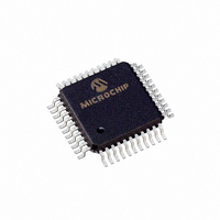
PIC17C42A-33I/PQ Microchip Technology, PIC17C42A-33I/PQ Datasheet - Page 62

PIC17C42A-33I/PQ
Manufacturer Part Number
PIC17C42A-33I/PQ
Description
IC MCU OTP 2KX16 PWM 44-MQFP
Manufacturer
Microchip Technology
Series
PIC® 17Cr
Datasheets
1.PIC16F616T-ISL.pdf
(8 pages)
2.PIC17C42A-16P.pdf
(241 pages)
3.PIC17C42A-16P.pdf
(4 pages)
Specifications of PIC17C42A-33I/PQ
Core Processor
PIC
Core Size
8-Bit
Speed
33MHz
Connectivity
UART/USART
Peripherals
POR, PWM, WDT
Number Of I /o
33
Program Memory Size
4KB (2K x 16)
Program Memory Type
OTP
Ram Size
232 x 8
Voltage - Supply (vcc/vdd)
4.5 V ~ 6 V
Oscillator Type
External
Operating Temperature
-40°C ~ 85°C
Package / Case
44-MQFP, 44-PQFP
Processor Series
PIC17C
Core
PIC
Data Bus Width
8 bit
Data Ram Size
232 B
Interface Type
SCI, USART
Maximum Clock Frequency
33 MHz
Number Of Programmable I/os
33
Number Of Timers
8
Operating Supply Voltage
2.5 V to 6 V
Maximum Operating Temperature
+ 85 C
Mounting Style
SMD/SMT
Development Tools By Supplier
ICE2000
Minimum Operating Temperature
- 40 C
For Use With
AC164316 - MODULE SKT MPLAB PM3 44MQFP
Lead Free Status / RoHS Status
Lead free / RoHS Compliant
Eeprom Size
-
Data Converters
-
Lead Free Status / Rohs Status
Details
Available stocks
Company
Part Number
Manufacturer
Quantity
Price
Company:
Part Number:
PIC17C42A-33I/PQ
Manufacturer:
Microchip Technology
Quantity:
10 000
- Current page: 62 of 241
- Download datasheet (2Mb)
PIC17C4X
9.4.1
PORTE is a 3-bit bi-directional port. The corresponding
data direction register is DDRE. A '1' in DDRE config-
ures the corresponding port pin as an input. A '0' in the
DDRE register configures the corresponding port pin
as an output. Reading PORTE reads the status of the
pins, whereas writing to it will write to the port latch.
PORTE is multiplexed with the system bus. When
operating as the system bus, PORTE contains the con-
trol signals for the address/data bus (AD15:AD0).
These control signals are Address Latch Enable (ALE),
Output Enable (OE), and Write (WR). The control sig-
nals OE and WR are active low signals. The timing for
the system bus is shown in the Electrical Characteris-
tics section.
FIGURE 9-8:
DS30412C-page 62
Note: I/O pins have protection diodes to V
Note:
PORTE AND DDRE REGISTER
This port is configured as the system bus
when the device’s configuration bits are
selected to Microprocessor or Extended
Microcontroller modes. In the two other
microcontroller modes, this port is a gen-
eral purpose I/O.
PORTE BLOCK DIAGRAM (IN I/O PORT MODE)
TTL
Input
Buffer
0
1
Data
Port
DD
and Vss.
R
Q
Q
CK
CK
S
D
D
Example 9-4 shows the instruction sequence to initial-
ize PORTE. The Bank Select Register (BSR) must be
selected to Bank 1 for the port to be initialized.
EXAMPLE 9-4:
MOVLB 1
CLRF
MOVLW 0x03
MOVWF DDRE
PORTE
INITIALIZING PORTE
;
;
;
;
;
;
;
;
;
;
;
Select Bank 1
Initialize PORTE data
Value used to initialize
Set RE<1:0> as inputs
1996 Microchip Technology Inc.
data direction
latches before setting
the data direction
register
RE<2> as outputs
RE<7:3> are always
read as '0'
WR_PORTE
RD_PORTE
WR_DDRE
RD_DDRE
DRV_SYS
Data Bus
EX_EN
CNTL
SYS BUS
Control
Related parts for PIC17C42A-33I/PQ
Image
Part Number
Description
Manufacturer
Datasheet
Request
R

Part Number:
Description:
IC,MICROCONTROLLER,8-BIT,PIC CPU,CMOS,LDCC,44PIN,PLASTIC
Manufacturer:
Microchip Technology
Datasheet:

Part Number:
Description:
IC MCU OTP 2KX16 PWM 40DIP
Manufacturer:
Microchip Technology
Datasheet:

Part Number:
Description:
IC MCU OTP 2KX16 PWM 40DIP
Manufacturer:
Microchip Technology
Datasheet:

Part Number:
Description:
IC MCU OTP 2KX16 PWM 44-MQFP
Manufacturer:
Microchip Technology
Datasheet:

Part Number:
Description:
IC MCU OTP 2KX16 PWM 44PLCC
Manufacturer:
Microchip Technology
Datasheet:

Part Number:
Description:
IC MCU OTP 2KX16 PWM 44PLCC
Manufacturer:
Microchip Technology
Datasheet:

Part Number:
Description:
IC MCU OTP 2KX16 PWM 44-MQFP
Manufacturer:
Microchip Technology
Datasheet:

Part Number:
Description:
IC MCU OTP 2KX16 PWM 44TQFP
Manufacturer:
Microchip Technology
Datasheet:

Part Number:
Description:
IC MCU OTP 2KX16 PWM 44TQFP
Manufacturer:
Microchip Technology
Datasheet:

Part Number:
Description:
IC MCU OTP 2KX16 PWM 40DIP
Manufacturer:
Microchip Technology
Datasheet:

Part Number:
Description:
IC MCU OTP 2KX16 PWM 40DIP
Manufacturer:
Microchip Technology
Datasheet:

Part Number:
Description:
IC MCU OTP 2KX16 PWM 40DIP
Manufacturer:
Microchip Technology
Datasheet:

Part Number:
Description:
IC MCU OTP 2KX16 PWM 44-MQFP
Manufacturer:
Microchip Technology
Datasheet:

Part Number:
Description:
IC MCU OTP 2KX16 PWM 44PLCC
Manufacturer:
Microchip Technology
Datasheet:

Part Number:
Description:
IC MCU OTP 2KX16 PWM 44-MQFP
Manufacturer:
Microchip Technology
Datasheet:


