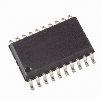
ATTINY2313-20SI Atmel, ATTINY2313-20SI Datasheet - Page 16

ATTINY2313-20SI
Manufacturer Part Number
ATTINY2313-20SI
Description
IC MCU AVR 2K FLASH 20SOIC
Manufacturer
Atmel
Series
AVR® ATtinyr
Specifications of ATTINY2313-20SI
Core Processor
AVR
Core Size
8-Bit
Speed
20MHz
Connectivity
SPI, UART/USART
Peripherals
Brown-out Detect/Reset, POR, PWM, WDT
Number Of I /o
18
Program Memory Size
2KB (1K x 16)
Program Memory Type
FLASH
Eeprom Size
128 x 8
Ram Size
128 x 8
Voltage - Supply (vcc/vdd)
2.7 V ~ 5.5 V
Oscillator Type
Internal
Operating Temperature
-40°C ~ 85°C
Package / Case
20-SOIC (7.5mm Width)
Lead Free Status / RoHS Status
Contains lead / RoHS non-compliant
Data Converters
-
Other names
ATTINY2313-24SI
ATTINY2313-24SI
ATTINY2313-24SI
Available stocks
Company
Part Number
Manufacturer
Quantity
Price
Company:
Part Number:
ATTINY2313-20SI
Manufacturer:
AT
Quantity:
95
Part Number:
ATTINY2313-20SI
Manufacturer:
RASTRONIC
Quantity:
20 000
- Current page: 16 of 226
- Download datasheet (4Mb)
EEPROM Data
Memory
EEPROM Read/Write
Access
The EEPROM Address
Register
16
ATtiny2313
Figure 10. On-chip Data SRAM Access Cycles
The ATtiny2313 contains 128 bytes of data EEPROM memory. It is organized as a separate
data space, in which single bytes can be read and written. The EEPROM has an endurance of at
least 100,000 write/erase cycles. The access between the EEPROM and the CPU is described
in the following, specifying the EEPROM Address Registers, the EEPROM Data Register, and
the EEPROM Control Register. For a detailed description of Serial data downloading to the
EEPROM, see
The EEPROM Access Registers are accessible in the I/O space.
The write access time for the EEPROM is given in
the user software detect when the next byte can be written. If the user code contains instructions
that write the EEPROM, some precautions must be taken. In heavily filtered power supplies, V
is likely to rise or fall slowly on power-up/down. This causes the device for some period of time to
run at a voltage lower than specified as minimum for the clock frequency used.
EEPROM Corruption” on page 20.
In order to prevent unintentional EEPROM writes, a specific write procedure must be followed.
Refer to the description of the EEPROM Control Register for details on this.
When the EEPROM is read, the CPU is halted for four clock cycles before the next instruction is
executed. When the EEPROM is written, the CPU is halted for two clock cycles before the next
instruction is executed.
• Bit 7 – Res: Reserved Bit
This bit is reserved in the ATtiny2313 and will always read as zero.
Bit
Read/Write
Initial Value
Address
clk
page
Data
Data
R
7
–
0
WR
CPU
RD
172.
EEAR6
R/W
X
6
Compute Address
EEAR5
R/W
X
5
T1
Memory Access Instruction
for details on how to avoid problems in these situations.
EEAR4
R/W
X
4
EEAR3
R/W
Address valid
3
X
Table
T2
EEAR2
R/W
2
X
1. A self-timing function, however, lets
EEAR1
R/W
Next Instruction
1
X
T3
EEAR0
R/W
0
X
See “Preventing
EEAR
2543L–AVR–08/10
CC
Related parts for ATTINY2313-20SI
Image
Part Number
Description
Manufacturer
Datasheet
Request
R

Part Number:
Description:
IC, MCU, 8BIT, 2K FLASH, 20SOIC
Manufacturer:
Atmel
Datasheet:

Part Number:
Description:
IC, MCU, 8BIT, 2K FLASH, 20PDIP
Manufacturer:
Atmel
Datasheet:

Part Number:
Description:
IC, MCU, 8BIT, 8K FLASH, 20PDIP
Manufacturer:
Atmel
Datasheet:

Part Number:
Description:
IC, MCU, 8BIT, 8K FLASH, 20SOIC
Manufacturer:
Atmel
Datasheet:

Part Number:
Description:
DEV KIT FOR AVR/AVR32
Manufacturer:
Atmel
Datasheet:

Part Number:
Description:
INTERVAL AND WIPE/WASH WIPER CONTROL IC WITH DELAY
Manufacturer:
ATMEL Corporation
Datasheet:

Part Number:
Description:
Low-Voltage Voice-Switched IC for Hands-Free Operation
Manufacturer:
ATMEL Corporation
Datasheet:

Part Number:
Description:
MONOLITHIC INTEGRATED FEATUREPHONE CIRCUIT
Manufacturer:
ATMEL Corporation
Datasheet:

Part Number:
Description:
AM-FM Receiver IC U4255BM-M
Manufacturer:
ATMEL Corporation
Datasheet:

Part Number:
Description:
Monolithic Integrated Feature Phone Circuit
Manufacturer:
ATMEL Corporation
Datasheet:

Part Number:
Description:
Multistandard Video-IF and Quasi Parallel Sound Processing
Manufacturer:
ATMEL Corporation
Datasheet:

Part Number:
Description:
High-performance EE PLD
Manufacturer:
ATMEL Corporation
Datasheet:


