AK4358VQ AKM Semiconductor Inc, AK4358VQ Datasheet
AK4358VQ
Specifications of AK4358VQ
Available stocks


Related parts for AK4358VQ


AK4358VQ Summary of contents
Page 1
The AK4358 is eight channels 24bit DAC corresponding to digital audio system. Using AKM's advanced multi bit architecture for its modulator the AK4358 delivers a wide dynamic range while preserving linearity for improved THD+N performance. The AK4358 has full differential ...
Page 2
... Ordering Guide -40 ∼ +85°C AK4358VQ AKD4358 Evaluation Board for AK4358 ■ Pin Layout LOUT1- LOUT1+ DZF3 DZF2 DZF1 CAD0 ACKSN PDN BICK MCLK 11 DVDD DVSS 12 MS0203-E-02 48LQFP AK4358VQ Top View [AK4358] 36 AVSS 35 AVDD 34 VREFH 33 ROUT4+ 32 ROUT4- 31 DIF0 30 DSDR3 29 DSDL3 28 DSDR2 ...
Page 3
Compatibility with AK4357 1. Function & Performance Functions # of channels DR 48kHz/96kHz TDM I2C DSDM control Input channel of DZF pin 2. Pin Configuration Pin # AK4357 3 DZFL1 4 DZFR1 5 DZF23 7 CAD1 ...
Page 4
No. Pin Name I/O 1 LOUT1 LOUT1 DZF3 O 4 DZF2 O 5 DZF1 O 6 CAD0 I 7 ACKSN I 8 PDN I 9 BICK I 10 MCLK I 11 DVDD - 12 DVSS - ...
Page 5
LOUT2 ROUT1 ROUT1+ O Note: All input pins except pull-down pin should not be left floating. (AVSS=DVSS=0V; Note 1) Parameter Power Supplies Analog Digital |AVSS-DVSS| Input Current (any pins except for supplies) Analog Input Voltage ...
Page 6
AVDD=DVDD=5V; VREFH=AVDD; fs=44.1kHz; BICK=64fs; Signal Frequency=1kHz; 24bit Input Data; Measurement frequency=20Hz ∼ 20kHz; R Parameter Resolution Dynamic Characteristics THD+N fs=44.1kHz BW=20kHz fs=96kHz BW=40kHz fs=192kHz BW=40kHz Dynamic Range (-60dBFS with A-weighted) S/N (A-weighted) Interchannel Isolation (1kHz) Interchannel Gain Mismatch DC ...
Page 7
SHARP ROLL-OFF FILTER CHARACTERISTICS (Ta = 25°C; AVDD=DVDD = 4.75 ∼ 5.25V 44.1kHz; DEM = OFF; SLOW = “0”; PCM Mode) Parameter Digital filter ±0.05dB Passband (Note -6.0dB Stopband (Note Passband Ripple Stopband Attenuation Group Delay (Note Digital ...
Page 8
AVDD=DVDD = 4.75 ∼ 5.25V; C Parameter Master Clock Frequency Duty Cycle LRCK Frequency Normal Mode (TDM0= “L”, TDM1= “L”) Normal Speed Mode Double Speed Mode Quad Speed Mode Duty Cycle TDM256 mode (TDM0= “H”, TDM1= “L”) ...
Page 9
Parameter Reset Timing PDN Pulse Width Note 16. BICK rising edge must not occur at the same time as LRCK edge. Note 17. DSD data transmitting device must meet this time. Note 18. Data must be held for sufficient time ...
Page 10
Timing Diagram MCLK LRCK BICK LRCK tBLR BICK SDTI MS0203-E-02 1/fCLK tCLKH tCLKL 1/fs tBCK tBCKH tBCKL Clock Timing tLRB tSDS tSDH Audio Serial Interface Timing (PCM Mode [AK4358] VIH VIL dCLK=tCLKH x fCLK, tCLKL x ...
Page 11
DCLK DSDL DSDR Audio Serial Interface Timing (DSD Normal Mode, DCKB = “0”) DCLK DSDL DSDR Audio Serial Interface Timing (DSD Phase Modulation Mode, DCKB = “0”) CSN tCSS CCLK CDTI MS0203-E-02 tDCK tDCKL tDCKH tDDD tDCK tDCKL tDCKH tDDD ...
Page 12
CSN CCLK CDTI D3 SDA tLOW tBUF SCL tHD:STA Stop Start PDN MS0203-E- WRITE Data Input Timing tR tHIGH tF tHD:DAT tSU:DAT tSU:STA Start Bus mode Timing tPD Power-down Timing - 12 - [AK4358] tCSW ...
Page 13
D/A Conversion Mode The AK4358 can perform D/A conversion for both PCM data and DSD data. When DSD mode, DSD data can be input from DCLK, DSDL1-4 and DSDR1-4 pins. When PCM mode, PCM data can be input from ...
Page 14
LRCK fs 128fs 88.2kHz 11.2896MHz 16.9344MHz 22.5792MHz 33.8688MHz 96.0kHz 12.2880MHz 18.4320MHz 24.5760MHz 36.8640MHz Table 4. System Clock Example (Double Speed Mode @Manual Setting Mode) LRCK fs 176.4kHz 192.0kHz Table 5. System Clock Example (Quad Speed Mode @Manual Setting Mode) LRCK ...
Page 15
Audio Serial Interface Format 1) PCM Mode When PCM mode, data is shifted in via the SDTI1-4 pins using BICK and LRCK inputs. The DIF0-2 as shown in 10 can select five serial data modes. Initial value of DIF0-2 ...
Page 16
LRCK BICK (64fs) SDTI Don’t care Mode 1 19:MSB, 0:LSB SDTI Don’t care 23 Mode 4 23:MSB, 0:LSB Lch Data LRCK BICK (64fs) SDTI 23 22 23:MSB, 0:LSB Lch Data LRCK 0 1 ...
Page 17
Mode TDM1 TDM0 DIF2 3/256fs (min) LRCK BICK(256fs) SDTI1( BICK 3/256fs (min) LRCK BICK(256fs) SDTI1( BICK 3/256fs (min) LRCK ...
Page 18
Mode TDM1 TDM0 DIF2 3/128fs (min) LRCK BICK(128fs) SDTI1( SDTI2( 3/128fs (min) LRCK BICK(128fs) SDTI1( SDTI2( 3/128fs (min) LRCK ...
Page 19
DSD Mode In case of DSD mode, DIF0-2 is ignored. The frequency of DCLK is fixed to 64fs. DCKB bit can invert the polarity of DCLK. DCLK (64fs) DCKB=1 DCLK (64fs) DCKB=0 DSDL,DSDR Normal DSDL,DSDR Phase Modulation ■ D/A ...
Page 20
De-emphasis Filter A digital de-emphasis filter is available for 32, 44.1 or 48kHz sampling rates (tc = 50/15µs) and is enabled or disabled with DEM0 and DEM1. In case of double speed and quad speed mode, the digital de-emphasis ...
Page 21
Zero Detection When the input data at all channels are continuously zeros for 8192 LRCK cycles, the AK4358 has Zero Detection like Table 16. DZF pin immediately goes to “L” if input data of each channel is not zero ...
Page 22
System Reset The AK4358 should be reset once by bringing PDN= ”L” upon power-up. The analog section exits power-down mode by MCLK input and then the digital section exits power-down mode after the internal counter counts MCLK during 4/fs. ...
Page 23
Reset Function When RSTN=0, DAC is powered down but the internal register values are not initialized. The analog outputs go to VCOM voltage and DZFL/DZFR pins go to “H”. RSTN bit Internal RSTN bit Internal Normal Operation State D/A ...
Page 24
Register Control Interface The AK4358 controls its functions via registers. 2 types of control mode write internal registers. In the I chip address is determined by the state of the CAD0 and CAD1 inputs. In 3-wire mode, the CAD1 ...
Page 25
I C-bus Control Mode (I2C= “H”) The AK4358 supports the standard-mode C-bus system (max: 400kHz). Figure 18 shows the data transfer sequence at the I HIGH to LOW transition on the SDA line while SCL ...
Page 26
SDA SCL S start condition DATA OUTPUT BY MASTER DATA OUTPUT BY SLAVE(AK4529) SCL FROM MASTER S START CONDITION SDA SCL MS0203-E-02 Figure 22. START and STOP conditions Figure 23. Acknowledge on the I data line change ...
Page 27
Register Map Addr Register Name 00H Control 1 01H Control 2 02H Speed & Power Down Control 03H De-emphasis Control 04H LOUT1 ATT Control 05H ROUT1 ATT Control 06H LOUT2 ATT Control 07H ROUT2 ATT Control 08H LOUT3 ATT ...
Page 28
Register Definitions Addr Register Name 00H Control 1 Default RSTN: Internal timing reset 0: Reset. All DZF pins go to “H” and any registers are not initialized. 1: Normal operation When MCLK frequency or DFS changes, the AK4358 should ...
Page 29
Addr Register Name 02H Speed & Power Down Control Default RSTN: Internal timing reset 0: Reset. All DZF pins go to “H” and any registers are not initialized. 1: Normal operation When MCLK frequency or DFS changes, the AK4358 should ...
Page 30
Addr Register Name 0AH Control 3 Default ATS1-0: DATT Speed Setting (See Initial: “00”, mode 0 DZFB: Inverting Enable of DZF 0: DZF goes “H” at Zero Detection 1: DZF goes “L” at Zero Detection DCKB: Polarity of DCLK (DSD ...
Page 31
Figure 25 shows the system connection diagram. An evaluation board (AKD4358) is available which demonstrates application circuits, the optimum layout, power supply arrangements and measurement results. + 10u 0.1u Reset Clock Gen 13 SDTI4 14 SDTI1 DSP 15 SDTI2 16 ...
Page 32
Digital Ground System Controller AVSS and DVSS must be connected to the same analog ground plane. 1. Grounding and Power Supply Decoupling AVDD and DVDD are usually supplied from analog supply in system and should be separated from system digital ...
Page 33
External Analog Filter It is recommended by SACD format book (Scarlet Book) that the filter response at SACD playback is an analog low pass filter with a cut-off frequency of maximum 50kHz and a slop of minimum 30dB/Oct. The ...
Page 34
LQFP(Unit:mm) 9.0 ± 0 0.22 ± 0.08 0.5 0.10 ■ Package & Lead frame material Package molding compound: Lead frame material: Lead frame surface treatment: MS0203-E-02 PACKAGE 7 0.10 M 0° ...
Page 35
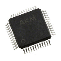
... MS0203-E-02 MARKING AKM AK4358VQ XXXXXXX 1 1) Asahi Kasei Logo 2) Marking Code: AK4358VQ 3) Date Code: XXXXXXX(7 digits) 4) Pin #1 indication Revision History Reason Page Contents First Edition Spec Change 8 SWITCHING CHARACTERISTICS TDM256 mode (TDM0= “H”, TDM1= “L”) tLRH (min): 1/256fs → 3/256fs tLRL (min): 1/256fs → ...
Page 36
These products and their specifications are subject to change without notice. When you consider any use or application of these products, please make inquiries the sales office of Asahi Kasei Microdevices Corporation (AKM) or authorized distributors as to current status ...