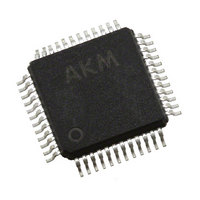
AK4358VQ AKM Semiconductor Inc, AK4358VQ Datasheet - Page 25

AK4358VQ
Manufacturer Part Number
AK4358VQ
Description
IC DAC 24BIT SERIAL 48LQFP
Manufacturer
AKM Semiconductor Inc
Datasheet
1.AK4358VQ.pdf
(36 pages)
Specifications of AK4358VQ
Number Of Bits
24
Data Interface
I²S, Serial
Number Of Converters
8
Voltage Supply Source
Analog and Digital
Operating Temperature
-40°C ~ 85°C
Mounting Type
Surface Mount
Package / Case
48-LFQFP
Lead Free Status / RoHS Status
Lead free / RoHS Compliant
Power Dissipation (max)
-
Settling Time
-
Other names
974-1008-2
Available stocks
Company
Part Number
Manufacturer
Quantity
Price
Company:
Part Number:
AK4358VQ
Manufacturer:
AKM Semiconductor Inc
Quantity:
1 951
Company:
Part Number:
AK4358VQ
Manufacturer:
AKM
Quantity:
11 050
Company:
Part Number:
AK4358VQ-L
Manufacturer:
ELPIDA
Quantity:
32
Part Number:
AK4358VQ-L
Manufacturer:
AKM
Quantity:
20 000
Company:
Part Number:
AK4358VQP-L
Manufacturer:
AKM Semiconductor Inc
Quantity:
10 000
MS0203-E-02
(2) I
The AK4358 supports the standard-mode I
I
Figure 18
HIGH to LOW transition on the SDA line while SCL is HIGH indicates a START condition
START condition, a slave address is sent. This address is 7 bits long followed by an eighth bit which is a data direction bit
(R/W)
and CAD0 (device address bits). These two bits identify the specific device on the bus. The hard-wired input pins (CAD1
pin and CAD0 pin) set them. If the slave address match that of the AK4358 and R/W bit is “0”, the AK4358 generates the
acknowledge and the write operation is executed. If R/W bit is “1”, the AK4358 generates the not acknowledge since the
AK4358 can be only a slave-receiver. The master must generate the acknowledge-related clock pulse and release the
SDA line (HIGH) during the acknowledge clock pulse
The second byte consists of the address for control registers of the AK4358. The format is MSB first, and those most
significant 3-bits are fixed to zeros
first, 8bits
always terminated by a STOP condition generated by the master. A LOW to HIGH transition on the SDA line while SCL
is HIGH defines a STOP condition
The AK4358 is capable of more than one byte write operation by one sequence. After receipt of the third byte, the
AK4358 generates an acknowledge, and awaits the next data again. The master can transmit more than one byte instead of
terminating the write cycle after the first data byte is transferred. After the receipt of each data, the internal 5bits address
counter is incremented by one, and the next data is taken into next address automatically. If the addresses exceed 1FH
prior to generating the stop condition, the address counter will “roll over” to 00H and the previous data will be
overwritten.
The data on the SDA line must be stable during the HIGH period of the clock. The HIGH or LOW state of the data line
can only change when the clock signal on the SCL line is LOW
condition.
2
C-bus system (max: 400kHz).
2
C-bus Control Mode (I2C= “H”)
(Figure
shows the data transfer sequence at the I
(Figure
SDA
19). The most significant five bits of the slave address are fixed as “00100”. The next two bits are CAD1
21). The AK4358 generates an acknowledge after each byte has been received. A data transfer is
D7
0
0
S
T
A
R
T
S
Slave
Address
Figure 18. Data transfer sequence at the I
D6
(Figure
(Those CAD1/0 should match with CAD1/0 pins)
0
0
(Figure
Figure 21. Byte structure after the second byte
R/W
A
C
K
2
20). Those data after the second byte contain control data. The format is MSB
Sub
Address(n)
22).
C-bus (max:100kHz). Then the AK4358 does not support a fast-mode
D5
1
0
Figure 20. The second byte
Figure 19. The first byte
2
C-bus mode. All commands are preceded by a START condition. A
A
C
K
A4
D4
0
(Figure
- 25 -
Data(n)
23).
(Figure
A3
D3
0
A
C
K
Data(n+1)
24) except for the START and the STOP
CAD1
2
A2
D2
C-bus mode
A
C
K
CAD0
A1
D1
A
C
K
Data(n+x)
R/W
A0
D0
(Figure
A
C
K
S
T
O
P
P
22). After the
[AK4358]
2009/05


