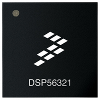
DSP56321VL275 Freescale Semiconductor, DSP56321VL275 Datasheet - Page 4

DSP56321VL275
Manufacturer Part Number
DSP56321VL275
Description
IC DSP 24BIT 275MHZ 196-MAPBGA
Manufacturer
Freescale Semiconductor
Series
DSP563xxr
Type
Fixed Pointr
Datasheet
1.DSP56321VL200R2.pdf
(84 pages)
Specifications of DSP56321VL275
Interface
Host Interface, SSI, SCI
Clock Rate
275MHz
Non-volatile Memory
ROM (576 B)
On-chip Ram
576kB
Voltage - I/o
3.30V
Voltage - Core
1.60V
Operating Temperature
-40°C ~ 100°C
Mounting Type
*
Package / Case
196-MAPBGA
Device Core Size
24b
Format
Fixed Point
Clock Freq (max)
275MHz
Mips
275
Device Input Clock Speed
275MHz
Ram Size
576KB
Operating Supply Voltage (typ)
1.6/3.3V
Operating Temp Range
-40C to 100C
Operating Temperature Classification
Industrial
Mounting
Surface Mount
Pin Count
196
Package Type
MA-BGA
Lead Free Status / RoHS Status
Lead free / RoHS Compliant
Available stocks
Company
Part Number
Manufacturer
Quantity
Price
Company:
Part Number:
DSP56321VL275
Manufacturer:
Freescale Semiconductor
Quantity:
10 000
Part Number:
DSP56321VL275
Manufacturer:
MOTOROLA/摩托罗拉
Quantity:
20 000
Target Applications
DSP56321 applications require high performance, low power, small packaging, and a large amount of internal
memory. The EFCOP can accelerate general filtering applications. Examples include:
iv
Power Dissipation
Internal Memories
External Memory
•
•
•
•
•
•
•
Expansion
Packaging
Wireless and wireline infrastructure applications
Multi-channel wireless local loop systems
Security encryption systems
Home entertainment systems
DSP resource boards
High-speed modem banks
IP telephony
Feature
:
• 192 × 24-bit bootstrap ROM
• 192 K × 24-bit RAM total
• Program RAM, instruction cache, X data RAM, and Y data RAM sizes are programmable:
• Data memory expansion to two 256 K × 24-bit word memory spaces using the standard external address
• Program memory expansion to one 256 K × 24-bit words memory space using the standard external
• External memory expansion port
• Chip select logic for glueless interface to static random access memory (SRAMs)
• Very low-power CMOS design
• Wait and Stop low-power standby modes
• Fully static design specified to operate down to 0 Hz (dc)
• Optimized power management circuitry (instruction-dependent, peripheral-dependent, and mode-
• Molded array plastic-ball grid array (MAP-BGA) package in lead-free or lead-bearing versions.
112 K × 24-bit
111 K × 24-bit
*Includes 12 K × 24-bit shared memory (that is, 24 K total memory shared by the core and the EFCOP)
Program RAM
32 K × 24-bit
31 K × 24-bit
40 K × 24-bit
39 K × 24-bit
48 K × 24-bit
47 K × 24-bit
64 K × 24-bit
63 K × 24-bit
72 K × 24-bit
71 K × 24-bit
80 K × 24-bit
79 K × 24-bit
96 K × 24-bit
95 K × 24-bit
lines
address lines
dependent)
Size
Table 1. DSP56321 Features (Continued)
1024 × 24-bit
1024 × 24-bit
1024 × 24-bit
1024 × 24-bit
1024 × 24-bit
1024 × 24-bit
1024 × 24-bit
1024 × 24-bit
DSP56321 Technical Data, Rev. 11
Cache Size
Instruction
0
0
0
0
0
0
0
0
80 K × 24-bit
80 K × 24-bit
76 K × 24-bit
76 K × 24-bit
72 K × 24-bit
72 K × 24-bit
64 K × 24-bit
64 K × 24-bit
60 K × 24-bit
60 K × 24-bit
56 K × 24-bit
56 K × 24-bit
48 K × 24-bit
48 K × 24-bit
40 K × 24-bit
40 K × 24-bit
X Data RAM
Size*
Description
80 K × 24-bit
80 K × 24-bit
76 K × 24-bit
76 K × 24-bit
72 K × 24-bit
72 K × 24-bit
64 K × 24-bit
64 K × 24-bit
60 K × 24-bit
60 K × 24-bit
56 K × 24-bit
56 K × 24-bit
48 K × 24-bit
48 K × 24-bit
40 K × 24-bit
40 K × 24-bit
Y Data RAM
Size*
Instruction
disabled
disabled
disabled
disabled
disabled
disabled
disabled
disabled
enabled
enabled
enabled
enabled
enabled
enabled
enabled
enabled
Cache
Freescale Semiconductor
MSW2
0
0
0
0
0
0
0
0
1
1
1
1
1
1
1
1
MSW1
0
0
0
0
1
1
1
1
0
0
0
0
1
1
1
1
MSW0
0
0
1
1
0
0
1
1
0
0
1
1
0
0
1
1


