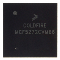
MCF5272CVM66 Freescale Semiconductor, MCF5272CVM66 Datasheet - Page 404

MCF5272CVM66
Manufacturer Part Number
MCF5272CVM66
Description
IC MPU 66MHZ COLDFIRE 196-MAPBGA
Manufacturer
Freescale Semiconductor
Series
MCF527xr
Specifications of MCF5272CVM66
Core Processor
Coldfire V2
Core Size
32-Bit
Speed
66MHz
Connectivity
EBI/EMI, Ethernet, I²C, SPI, UART/USART, USB
Peripherals
DMA, WDT
Number Of I /o
32
Program Memory Size
16KB (4K x 32)
Program Memory Type
ROM
Ram Size
1K x 32
Voltage - Supply (vcc/vdd)
3 V ~ 3.6 V
Oscillator Type
External
Operating Temperature
-40°C ~ 85°C
Package / Case
196-MAPBGA
Cpu Speed
66MHz
Embedded Interface Type
UART, QSPI, USB, TDM
Digital Ic Case Style
BGA
No. Of Pins
196
Supply Voltage Range
3V To 3.6V
Rohs Compliant
Yes
Family Name
MCF5xxx
Device Core
ColdFire
Device Core Size
32b
Frequency (max)
66MHz
Instruction Set Architecture
RISC
Supply Voltage 1 (typ)
3.3V
Operating Temp Range
-40C to 85C
Operating Temperature Classification
Industrial
Mounting
Surface Mount
Pin Count
196
Package Type
MA-BGA
Lead Free Status / RoHS Status
Lead free / RoHS Compliant
Eeprom Size
-
Data Converters
-
Lead Free Status / Rohs Status
Compliant
Available stocks
Company
Part Number
Manufacturer
Quantity
Price
Company:
Part Number:
MCF5272CVM66
Manufacturer:
MOT
Quantity:
3
Company:
Part Number:
MCF5272CVM66
Manufacturer:
Freescale Semiconductor
Quantity:
10 000
Part Number:
MCF5272CVM66
Manufacturer:
FREESCALE
Quantity:
20 000
Company:
Part Number:
MCF5272CVM66J
Manufacturer:
NSC
Quantity:
36
Company:
Part Number:
MCF5272CVM66J
Manufacturer:
Freescale Semiconductor
Quantity:
10 000
- Current page: 404 of 544
- Download datasheet (7Mb)
General Purpose I/O Module
17.3
These registers are used to program GPIO port signals as inputs or outputs. The data direction bit for any
line is ignored unless that line is configured for general purpose I/O in the appropriate control register. If
a GPIO line changes from an input to an output, the initial data on that pin is the last data written to the
latch by the corresponding data register.
At system reset, these register bits are all cleared, configuring all port I/O lines as general purpose inputs.
Bootstrap software must write an appropriate value into the data direction register to configure GPIO port
signals as outputs. When these registers are first written, any internal pullups on the corresponding I/O pins
are disabled.
A detailed description is provided only for data direction register A (PADDR). The control bits in all three
registers operate in the same manner.
17.3.1
The PADDR determines the signal direction of each parallel port pin programmed as a GPIO port in the
PACNT.
17.3.2
The PBDDR determines the signal direction of each parallel port pin programmed as a GPIO port in the
PBCNT.
17-10
15–0
Bits
Reset
Reset
Field
Field
Addr
Addr
R/W
R/W
Data Direction Registers
15
15
Port A Data Direction Register (PADDR)
Port B Data Direction Register (PBDDR)
PADDR
Name
MCF5272 ColdFire
Data direction bits. Each data direction bit selects the direction of the signal as follows:
0 Signal is defined as an input.
1 Signal is defined as an output.
Figure 17-5. Port B Data Direction Register (PBDDR)
Figure 17-4. Port A Data Direction Register (PADDR)
Table 17-9. PADDR Field Descriptions
®
Integrated Microprocessor User’s Manual, Rev. 3
0000_0000_0000_0000
0000_0000_0000_0000
MBAR + 0x008C
MBAR + 0x0084
Read/Write
Read/Write
PBDDR
PADDR
Description
Freescale Semiconductor
0
0
Related parts for MCF5272CVM66
Image
Part Number
Description
Manufacturer
Datasheet
Request
R
Part Number:
Description:
Mcf5272 Coldfire Integrated Microprocessor User
Manufacturer:
Freescale Semiconductor, Inc
Datasheet:

Part Number:
Description:
MCF5272 Interrupt Service Routine for the Physical Layer Interface Controller
Manufacturer:
Freescale Semiconductor / Motorola
Datasheet:
Part Number:
Description:
Manufacturer:
Freescale Semiconductor, Inc
Datasheet:
Part Number:
Description:
Manufacturer:
Freescale Semiconductor, Inc
Datasheet:
Part Number:
Description:
Manufacturer:
Freescale Semiconductor, Inc
Datasheet:
Part Number:
Description:
Manufacturer:
Freescale Semiconductor, Inc
Datasheet:
Part Number:
Description:
Manufacturer:
Freescale Semiconductor, Inc
Datasheet:
Part Number:
Description:
Manufacturer:
Freescale Semiconductor, Inc
Datasheet:
Part Number:
Description:
Manufacturer:
Freescale Semiconductor, Inc
Datasheet:
Part Number:
Description:
Manufacturer:
Freescale Semiconductor, Inc
Datasheet:
Part Number:
Description:
Manufacturer:
Freescale Semiconductor, Inc
Datasheet:
Part Number:
Description:
Manufacturer:
Freescale Semiconductor, Inc
Datasheet:
Part Number:
Description:
Manufacturer:
Freescale Semiconductor, Inc
Datasheet:
Part Number:
Description:
Manufacturer:
Freescale Semiconductor, Inc
Datasheet:
Part Number:
Description:
Manufacturer:
Freescale Semiconductor, Inc
Datasheet:


