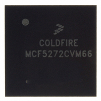
MCF5272CVM66 Freescale Semiconductor, MCF5272CVM66 Datasheet - Page 434

MCF5272CVM66
Manufacturer Part Number
MCF5272CVM66
Description
IC MPU 66MHZ COLDFIRE 196-MAPBGA
Manufacturer
Freescale Semiconductor
Series
MCF527xr
Specifications of MCF5272CVM66
Core Processor
Coldfire V2
Core Size
32-Bit
Speed
66MHz
Connectivity
EBI/EMI, Ethernet, I²C, SPI, UART/USART, USB
Peripherals
DMA, WDT
Number Of I /o
32
Program Memory Size
16KB (4K x 32)
Program Memory Type
ROM
Ram Size
1K x 32
Voltage - Supply (vcc/vdd)
3 V ~ 3.6 V
Oscillator Type
External
Operating Temperature
-40°C ~ 85°C
Package / Case
196-MAPBGA
Cpu Speed
66MHz
Embedded Interface Type
UART, QSPI, USB, TDM
Digital Ic Case Style
BGA
No. Of Pins
196
Supply Voltage Range
3V To 3.6V
Rohs Compliant
Yes
Family Name
MCF5xxx
Device Core
ColdFire
Device Core Size
32b
Frequency (max)
66MHz
Instruction Set Architecture
RISC
Supply Voltage 1 (typ)
3.3V
Operating Temp Range
-40C to 85C
Operating Temperature Classification
Industrial
Mounting
Surface Mount
Pin Count
196
Package Type
MA-BGA
Lead Free Status / RoHS Status
Lead free / RoHS Compliant
Eeprom Size
-
Data Converters
-
Lead Free Status / Rohs Status
Compliant
Available stocks
Company
Part Number
Manufacturer
Quantity
Price
Company:
Part Number:
MCF5272CVM66
Manufacturer:
MOT
Quantity:
3
Company:
Part Number:
MCF5272CVM66
Manufacturer:
Freescale Semiconductor
Quantity:
10 000
Part Number:
MCF5272CVM66
Manufacturer:
FREESCALE
Quantity:
20 000
Company:
Part Number:
MCF5272CVM66J
Manufacturer:
NSC
Quantity:
36
Company:
Part Number:
MCF5272CVM66J
Manufacturer:
Freescale Semiconductor
Quantity:
10 000
- Current page: 434 of 544
- Download datasheet (7Mb)
Signal Descriptions
After a device reset, INT[4:1] are enabled but the function is masked. INT4/DIN3 function can be changed
by software. INT[3:1] functions are always assigned to dedicated pins.
Interrupts INT[6:4] are multiplexed with other functions as follows:
INT1 is also internally connected to the USC_WOR function.
The INT6 function is always available regardless of the other functions enabled on this pin.
19.9
Each of the three GPIO ports is 16 bits wide. Each port line can be individually configured as input or
output. Except where indicated, each pin function is independently selectable between the corresponding
port pin or the other functions that may be multiplexed onto the pin. After reset all pins multiplexed with
GPIO signals default to inputs.
Port A general purpose I/O, PA[15:8] are multiplexed with PLIC TDM port 1 pins.
Port A general purpose I/O, PA[6:0] are multiplexed with USB module signals. PA7 is multiplexed with
QSPI_CS3 and DOUT3.
Port B general purpose I/O, PB[4:0] are multiplexed with the UART0 interface pins. If the UART0
interface is enabled, PB[4:0] are unavailable. PB5 is multiplexed with TA. PB6 is dedicated. PB7 is
multiplexed with TOUT0.
Port B general purpose I/O, PB[15:8] are multiplexed with the Ethernet interface pins. If the Ethernet
interface is enabled, PB[15:8] are unavailable.
Port C general purpose I/O, PC[15:0] are multiplexed with D[15:0]. When 32-bit wide bus mode is
selected, port C is unavailable.
19.10 UART0 Module Signals and PB[4:0]
The UART0 module uses the signals in this section for data and clock signals.
These signals are multiplexed with the GPIO port B signals PB[4:0].
19.10.1 Transmit Serial Data Output (URT0_TxD/PB0)
UART0 mode: URT0_TxD is the transmitter serial data output for the UART0 module. The output is held
high (mark condition) when the transmitter is disabled, idle, or in the local loopback mode. Data is shifted
out, lsb first, on this pin at the falling edge of the serial clock source.
Port B mode: This pin can also be configured as the PB0 I/O.
19-24
•
•
•
DGNT1_INT6/PA15_INT6
INT5/URT1_RTS
INT4/DIN3
General-Purpose I/O (GPIO) Ports
MCF5272 ColdFire
®
Integrated Microprocessor User’s Manual, Rev. 3
Freescale Semiconductor
Related parts for MCF5272CVM66
Image
Part Number
Description
Manufacturer
Datasheet
Request
R
Part Number:
Description:
Mcf5272 Coldfire Integrated Microprocessor User
Manufacturer:
Freescale Semiconductor, Inc
Datasheet:

Part Number:
Description:
MCF5272 Interrupt Service Routine for the Physical Layer Interface Controller
Manufacturer:
Freescale Semiconductor / Motorola
Datasheet:
Part Number:
Description:
Manufacturer:
Freescale Semiconductor, Inc
Datasheet:
Part Number:
Description:
Manufacturer:
Freescale Semiconductor, Inc
Datasheet:
Part Number:
Description:
Manufacturer:
Freescale Semiconductor, Inc
Datasheet:
Part Number:
Description:
Manufacturer:
Freescale Semiconductor, Inc
Datasheet:
Part Number:
Description:
Manufacturer:
Freescale Semiconductor, Inc
Datasheet:
Part Number:
Description:
Manufacturer:
Freescale Semiconductor, Inc
Datasheet:
Part Number:
Description:
Manufacturer:
Freescale Semiconductor, Inc
Datasheet:
Part Number:
Description:
Manufacturer:
Freescale Semiconductor, Inc
Datasheet:
Part Number:
Description:
Manufacturer:
Freescale Semiconductor, Inc
Datasheet:
Part Number:
Description:
Manufacturer:
Freescale Semiconductor, Inc
Datasheet:
Part Number:
Description:
Manufacturer:
Freescale Semiconductor, Inc
Datasheet:
Part Number:
Description:
Manufacturer:
Freescale Semiconductor, Inc
Datasheet:
Part Number:
Description:
Manufacturer:
Freescale Semiconductor, Inc
Datasheet:


