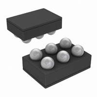
LMH2100TM/NOPB National Semiconductor, LMH2100TM/NOPB Datasheet - Page 2

LMH2100TM/NOPB
Manufacturer Part Number
LMH2100TM/NOPB
Description
IC LOG DETECTOR 4GHZ 40DB 6MSMD
Manufacturer
National Semiconductor
Datasheet
1.LMH2100TMNOPB.pdf
(32 pages)
Specifications of LMH2100TM/NOPB
Frequency
50MHz ~ 4GHz
Rf Type
Cellular, W-CDMA, CDMA, GSM, UMTS
Input Range
-45dBm ~ -5dBm
Accuracy
0.5dB
Voltage - Supply
2.7 V ~ 3.3 V
Current - Supply
9.2mA
Package / Case
6-UFBGA
Pin Count
6
Screening Level
Industrial
Lead Free Status / RoHS Status
Lead free / RoHS Compliant
Other names
LMH2100TMTR
www.national.com
Supply Interface
I
Logic Enable Interface
V
V
I
RF Input Interface
R
Output Interface
V
I
BW
R
SR
R
DD
EN
OUT
Symbol
LOW
HIGH
OUT
IN
TRANS
OUT
Absolute Maximum Ratings
If Military/Aerospace specified devices are required,
please contact the National Semiconductor Sales Office/
Distributors for availability and specifications.
2.7 V DC and AC Electrical Characteristics
Unless otherwise specified, all limits are guaranteed at T
Wave, unmodulated). Boldface limits apply at the temperature extremes (Note 4).
Supply Voltage
RF Input
Enable Input Voltage
ESD Tolerance (Note 2)
Storage Temperature
Range
V
Input power
DC Voltage
Human Body Model
Machine Model
Charge Device Model
DD
- GND
Supply Current
EN Logic Low Input Level
(Shutdown Mode)
EN Logic High Input Level
Current into EN Pin
Input Resistance
Output Voltage Swing
Output Short Circuit Current
Small Signal Bandwidth
Output Amp Transimpedance
Gain
Slew Rate
Output Impedance
(Note 8)
Parameter
V
SS
- 0.4V < V
EN
−65°C to 150°C
Active mode: EN = High, no signal
present at RF
Shutdown: EN = Low, no signal present
at RF
EN = Low: P
From Positive Rail, Sourcing,
V
From Negative Rail, Sinking,
V
Sourcing, V
Sinking, V
No RF input signal. Measured from REF
input current to V
No RF input signal, from I
DC
Positive, V
Negative, V
No RF input signal, EN = High. DC
measurement
< V
REF
REF
(Note 1)
DD
= 0V, I
= 2.7V, I
IN
10 dBm
400 mV
.
+ 0.4V
2000V
2000V
200V
3.6V
REF
REF
A
REF
REF
OUT
IN
= 25°C, V
IN
OUT
= 2.7V, V
Condition
from 2.7V to 0V
= 0 dBm (Note 8)
.
= 0V, V
from 0V to 2.7V
= 1 mA
OUT
= 1 mA
2
OUT
Supply Voltage
Temperature Range
RF Frequency Range
RF Input Power Range (Note 5)
Package Thermal Resistance θ
(Note 3)
DD
OUT
Operating Ratings
Junction Temperature
(Note 3)
Maximum Lead Temperature
REF
= 2.7V, RF input frequency f = 1855 MHz CW (Continuous
= 2.6V
(Soldering,10 sec)
= 0.1V
to V
OUT
,
(Note 6)
46.7
40.7
Min
6.3
5.0
1.1
5.8
5.2
6.2
5.4
3.4
3.3
3.8
3.7
(Note 7)
JA
51.5
15.3
13.1
43.3
Typ
416
7.1
0.5
7.3
8.3
3.9
4.4
0.2
(Note 1)
−58 dBV to −18 dBV
−45 dBm to −5 dBm
(Note 6)
50 MHz to 4 GHz
Max
56.4
23.9
28.9
22.3
28.3
46.7
7.9
9.2
0.9
1.9
0.6
1.8
4.0
10
50
−40°C to +85°C
2.7V to 3.3V
126.3°C/W
150°C
260°C
Units
V/µs
kHz
mA
mV
mA
μA
nA
kΩ
V
V
Ω
Ω


