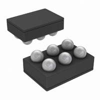
LMH2100TM/NOPB National Semiconductor, LMH2100TM/NOPB Datasheet - Page 26

LMH2100TM/NOPB
Manufacturer Part Number
LMH2100TM/NOPB
Description
IC LOG DETECTOR 4GHZ 40DB 6MSMD
Manufacturer
National Semiconductor
Datasheet
1.LMH2100TMNOPB.pdf
(32 pages)
Specifications of LMH2100TM/NOPB
Frequency
50MHz ~ 4GHz
Rf Type
Cellular, W-CDMA, CDMA, GSM, UMTS
Input Range
-45dBm ~ -5dBm
Accuracy
0.5dB
Voltage - Supply
2.7 V ~ 3.3 V
Current - Supply
9.2mA
Package / Case
6-UFBGA
Pin Count
6
Screening Level
Industrial
Lead Free Status / RoHS Status
Lead free / RoHS Compliant
Other names
LMH2100TMTR
www.national.com
In a practical power measurement system, temperature com-
pensation is usually only applied to a small power range
around the maximum power level for two reasons:
•
•
The table in the datasheet specifies the temperature sensi-
tivity for the aforementioned two segments at an input power
level of −10 dBm (near the top-end of the detector dynamic
range). The typical value represents the mean which is to be
used for calibration.
2.5 Differential Power Errors
Many third generation communication systems contain a
power control loop through the base station and mobile unit
that requests both to frequently update the transmit power
level by a small amount (typically 1 dB). For such applications
it is important that the actual change of the transmit power is
sufficiently close to the requested power change.
The error metrics in the datasheet that describe the accuracy
of the detector for a change in the input power are E
a 1 dB change in the input power) and E
or ten consecutive steps of 1 dB). Since it can be assumed
that the temperature does not change during the power step
The core of the LMH2100 is a progressive compression LOG-
detector consisting of four gain stages. Each of these satu-
rating stages has a gain of approximately 10 dB and therefore
realizes about 10 dB of the detector dynamic range. The five
diode cells perform the actual detection and convert the RF
signal to a DC current. This DC current is subsequently sup-
plied to the transimpedance amplifier at the output, that con-
verts it into an output voltage. In addition, the amplifier
provides buffering of and applies filtering to the detector out-
put signal. To prevent discharge of filtering capacitors be-
tween OUT and GND in shutdown, a switch is inserted at the
amplifier input that opens in shutdown to realize a high
impedance output of the device.
3.2 RF Input
RF parts typically use a characteristic impedance of 50Ω. To
comply with this standard the LMH2100 has an input
impedance of 50Ω. Using a characteristic impedance other
then 50Ω will cause a shift of the logarithmic intercept with
The various communication standards require the highest
accuracy in this range to limit interference.
The temperature sensitivity itself is a function of the power
level it becomes impractical to store a large number of
different temperature sensitivity values for different power
levels.
10 dB
FIGURE 10. Block Diagram of the LMH2100
(for a 10 dB step,
1 dB
(for
26
the differential error equals the difference of the drift error at
the two involved power levels:
It should be noted that the step error increases significantly
when one (or both) power levels in the above expression are
outside the detector dynamic range. For E
when P
of the dynamic range, P
3.0 DETECTOR INTERFACING
For optimal performance of the LMH2100, it is important that
all its pins are connected to the surrounding circuitry in the
appropriate way. This section discusses guidelines and re-
quirements for the electrical connection of each pin of the
LMH2100 to ensure proper operation of the device. Starting
from a block diagram, the function of each pin is elaborated.
Subsequently, the details of the electrical interfacing are sep-
arately discussed for each pin. Special attention will be paid
to the output filtering options and the differences between
single ended and differential interfacing with an ADC.
3.1 Block Diagram of the LMH2100
The block diagram of the LMH2100 is depicted in Figure 10.
respect to the value given in the electrical characteristics ta-
ble. This intercept shift can be calculated according to the
following formula: .
The intercept will shift to higher power levels for
R
R
3.3 Shutdown
To save power, the LMH2100 can be brought into a low-power
shutdown mode. The device is active for EN = HIGH
(V
LOW (V
switched to a high impedance mode. Using the shutdown
SOURCE
SOURCE
EN
>1.1V) and in the low-power shutdown mode for EN =
IN
EN
< 50Ω.
is less than 10 dB below the maximum input power
> 50Ω, and will shift to lower power levels for
< 0.6V). In this state the output of the LMH2100 is
30014003
MAX
.
10 dB
this occurs


