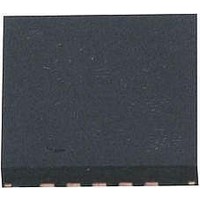
AT42QT1070-MMH Atmel, AT42QT1070-MMH Datasheet - Page 18

AT42QT1070-MMH
Manufacturer Part Number
AT42QT1070-MMH
Description
IC TOUCH SENSOR 7KEY 20-VQFN
Manufacturer
Atmel
Type
Capacitiver
Specifications of AT42QT1070-MMH
Number Of Inputs/keys
7 Key (Comms), 5 Key (Standalone)
Data Interface
I²C
Voltage Reference
Internal
Voltage - Supply
1.8 V ~ 5.5 V
Operating Temperature
-40°C ~ 85°C
Mounting Type
Surface Mount
Package / Case
20-VFQFN Exposed Pad
Supply Voltage
1.8 V to 5.5 V
Dimensions
3 mm L x 3 mm W x 0.8 mm H
Temperature Range
- 40 C to + 85 C
Termination Style
SMD/SMT
Lead Free Status / RoHS Status
Lead free / RoHS Compliant
Current - Supply
-
Resolution (bits)
-
Touch Panel Interface
-
Data Rate/sampling Rate (sps, Bps)
-
Lead Free Status / Rohs Status
Lead free / RoHS Compliant
Available stocks
Company
Part Number
Manufacturer
Quantity
Price
Company:
Part Number:
AT42QT1070-MMH QS529
Manufacturer:
Atmel
Quantity:
9 390
10620D–AT42–04/09
General Advice
2.5
2-8
Electrostatic Discharge Protection
Any LED terminal already connected full time to either Vdd or ground, even if through a limiting resistor,
does not need such bypassing. LEDs that are constantly driven (for example, just for constant
backlighting) do not normally require bypassing so long as these LEDs are driven before the control chip
is given a chance to calibrate itself on power-up. Multiplexed LEDs usually require bypassing on one
terminal but since multiplex lines drive two or more LEDs, the number of bypass capacitors need not be
one per LED; only one capacitor per common drive line is needed.
Other kinds of signal traces that change impedance can also cause false detections. Any nearby trace
that switches between “floating” and “clamped” states will usually cause a slight apparent capacitance
change and should be bypassed. Push-pull driven traces, so long as they are never three state, do not
require bypassing.
In general, Atmel capacitive sensors do not need extra ESD protection on their electrodes or traces.
Normally, the touch sensor is located behind a dielectric panel that has a breakdown potential of tens of
kilovolts per mm of thickness.
The single greatest threat from ESD tends to occur where there is a gap or hole in the panel, particularly
at the edge of the panel. In these situations an effect known as "creepage" can allow ESD to track
across an insulating surface and connect directly with the sensor or interconnecting tracks
Figure 2-4.
Places to watch for ESD creepage also include regions where flex circuits or tails pass close to a panel
gap (see
Figure
Touch Sensor
Electrode
Behind Panel
Effect of ESD Creepage
2-5).
PCB
ESD can track across
the surface and “zap”
the sensor directly
on the rear of the panel
ESD Strike Here
Touch Sensors Design Guide
Hole In Panel
Overlying Panel
(Figure
2-4).


