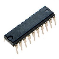
ATTINY461V-10PU Atmel, ATTINY461V-10PU Datasheet - Page 117

ATTINY461V-10PU
Manufacturer Part Number
ATTINY461V-10PU
Description
Microcontrollers (MCU) 4kB Flash 0.256kB EEPROM 16 I/O Pins
Manufacturer
Atmel
Specifications of ATTINY461V-10PU
Processor Series
ATTINY4x
Core
AVR8
Data Bus Width
8 bit
Data Ram Size
256 B
Interface Type
2-Wire/SPI/USI
Maximum Clock Frequency
10 MHz
Number Of Programmable I/os
16
Number Of Timers
2
Operating Supply Voltage
2.7 V to 5.5 V
Maximum Operating Temperature
+ 85 C
Mounting Style
Through Hole
Minimum Operating Temperature
- 40 C
On-chip Adc
11-ch x 10-bit
Program Memory Type
Flash
Program Memory Size
4 KB
Package / Case
PDIP-20
Package
20PDIP
Device Core
AVR
Family Name
ATtiny
Maximum Speed
10 MHz
Ram Size
256 Byte
Operating Temperature
-40 to 85 °C
Lead Free Status / RoHS Status
Lead free / RoHS Compliant
Available stocks
Company
Part Number
Manufacturer
Quantity
Price
Company:
Part Number:
ATTINY461V-10PU
Manufacturer:
ATMEL
Quantity:
6 223
- Current page: 117 of 242
- Download datasheet (5Mb)
12.12.3
2588E–AVR–08/10
TCCR1C – Timer/Counter1 Control Register C
• Bits 7,6 – COM1A1S, COM1A0S: Comparator A Output Mode, Shadow Bits 1 and 0
These are shadow bits of COM1A1 and COM1A0 in TCCR1A. Writing to bits COM1A1S and
COM1A0S will also change bits COM1A1 and COM1A0 in TCCR1A. Similary, changes written
to bits COM1A1 and COM1A0 in TCCR1A will show here.
See
• Bits 5,4 – COM1B1S, COM1B0S: Comparator B Output Mode, Shadow Bits 1 and 0
These are shadow bits of COM1B1 and COM1B0 in TCCR1A. Writing to bits COM1B1S and
COM1B0S will also change bits COM1B1 and COM1B0 in TCCR1A. Similary, changes written
to bits COM1B1 and COM1B0 in TCCR1A will show here.
See
• Bits 3,2 – COM1D1, COM1D0: Comparator D Output Mode, Bits 1 and 0
These bits control the behaviour of the Waveform Output (OCW1D) and the connection of the
Output Compare pin (OC1D). If one or both of the COM1D1:0 bits are set, the OC1D output
overrides the normal port functionality of the I/O pin it is connected to. The complementary
OC1D output is connected only in PWM modes when the COM1D1:0 bits are set to “01”. Note
that the Data Direction Register (DDR) bit corresponding to the OC1D pin must be set in order to
enable the output driver.
The function of the COM1D1:0 bits depends on the PWM1D and WGM11:10 bit settings.
12-18
PWM).
Table 12-18. Compare Output Mode, Normal Mode (non-PWM)
Table 12-19
set to Fast PWM Mode.
Table 12-19. Compare Output Mode, Fast PWM Mode
Bit
0x27 (0x47)
Read/Write
Initial value
COM1D1:0
COM1D1:0
“TCCR1A – Timer/Counter1 Control Register A” on page 112
“TCCR1A – Timer/Counter1 Control Register A” on page 112
00
01
10
11
00
01
10
11
shows the COM1D1:0 bit functionality when the PWM1D bit is set to a Normal Mode (non-
shows the COM1D1:0 bit functionality when the PWM1D and WGM11:10 bits are
COM1A1
OCW1D Behaviour
Normal port operation.
Cleared on Compare Match. Set when TCNT1=0x000.
Cleared on Compare Match. Set when TCNT1=0x000.
Set on Compare Match. Cleared when TCNT1=0x000.
R/W
OCW1D Behaviour
Normal port operation.
Toggle on Compare Match.
Clear on Compare Match.
Set on Compare Match.
S
7
0
COM1A0
R/W
S
6
0
COM1B1
R/W
S
5
0
COM1B0
R/W
S
4
0
COM1D1
R/W
3
0
COM1D0
R/W
2
0
OC1D Pin
Disconnected
Connected
Connected
Connected
OC1D Pin
Disconnected
Connected
Connected
Connected
for information on bit usage.
for information on bit usage.
FOC1D
R/W
1
0
PWM1D
R/W
OC1D Pin
Disconnected
Disconnected
Disconnected
Disconnected
0
0
Disconnected
Disconnected
OC1D Pin
Disconnected
Connected
TCCR1C
Table
117
Related parts for ATTINY461V-10PU
Image
Part Number
Description
Manufacturer
Datasheet
Request
R

Part Number:
Description:
Manufacturer:
Atmel Corporation
Datasheet:

Part Number:
Description:
Manufacturer:
Atmel Corporation
Datasheet:

Part Number:
Description:
IC AVR MCU 4K 20MHZ 32-QFN
Manufacturer:
Atmel
Datasheet:

Part Number:
Description:
IC MCU AVR 4K FLASH 20MHZ 20SOIC
Manufacturer:
Atmel
Datasheet:

Part Number:
Description:
MCU AVR 4K FLASH 15MHZ 32-QFN
Manufacturer:
Atmel
Datasheet:

Part Number:
Description:
MCU AVR 4KB FLASH 15MHZ 32-VQFN
Manufacturer:
Atmel
Datasheet:

Part Number:
Description:
MCU AVR 4KB FLASH 20MHZ 20SOIC
Manufacturer:
Atmel
Datasheet:

Part Number:
Description:
IC MCU AVR 4K 20MHZ 32QFN
Manufacturer:
Atmel
Datasheet:

Part Number:
Description:
Microcontrollers (MCU) 4kB Flash 0.256kB EEPROM 16 I/O Pins
Manufacturer:
Atmel
Datasheet:

Part Number:
Description:
IC, MCU, 8BIT, 2K FLASH, 20SOIC
Manufacturer:
Atmel
Datasheet:


