ATTINY461V-10PU Atmel, ATTINY461V-10PU Datasheet - Page 153
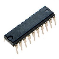
ATTINY461V-10PU
Manufacturer Part Number
ATTINY461V-10PU
Description
Microcontrollers (MCU) 4kB Flash 0.256kB EEPROM 16 I/O Pins
Manufacturer
Atmel
Specifications of ATTINY461V-10PU
Processor Series
ATTINY4x
Core
AVR8
Data Bus Width
8 bit
Data Ram Size
256 B
Interface Type
2-Wire/SPI/USI
Maximum Clock Frequency
10 MHz
Number Of Programmable I/os
16
Number Of Timers
2
Operating Supply Voltage
2.7 V to 5.5 V
Maximum Operating Temperature
+ 85 C
Mounting Style
Through Hole
Minimum Operating Temperature
- 40 C
On-chip Adc
11-ch x 10-bit
Program Memory Type
Flash
Program Memory Size
4 KB
Package / Case
PDIP-20
Package
20PDIP
Device Core
AVR
Family Name
ATtiny
Maximum Speed
10 MHz
Ram Size
256 Byte
Operating Temperature
-40 to 85 °C
Lead Free Status / RoHS Status
Lead free / RoHS Compliant
Available stocks
Company
Part Number
Manufacturer
Quantity
Price
Company:

Part Number:
ATTINY461V-10PU
Manufacturer:
ATMEL
Quantity:
6 223


15.11 ADC Conversion Result
15.11.1
2588E–AVR–08/10
Single Ended Conversion
Figure 15-12. Differential Non-linearity (DNL)
After the conversion is complete (ADIF is high), the conversion result can be found in the ADC
Result Registers (ADCL, ADCH). The form of the conversion result depends on the type of the
conversio as there are three types of conversions: single ended conversion, unipolar differential
conversion and bipolar differential conversion.
For single ended conversion, the result is
where V
Table 15-3 on page 155
• Differential Non-linearity (DNL): The maximum deviation of the actual code width (the interval
• Quantization Error: Due to the quantization of the input voltage into a finite number of codes,
• Absolute Accuracy: The maximum deviation of an actual (unadjusted) transition compared to
between two adjacent transitions) from the ideal code width (1 LSB). Ideal value: 0 LSB.
a range of input voltages (1 LSB wide) will code to the same value. Always ± 0.5 LSB.
an ideal transition for any code. This is the compound effect of offset, gain error, differential
error, non-linearity, and quantization error. Ideal value: ± 0.5 LSB.
Output Code
IN
is the voltage on the selected input pin and V
0x000
0x3FF
0
and
1 LSB
Table 15-4 on page
ADC
=
V
--------------------------
IN
V
⋅
REF
1024
157). 0x000 represents analog ground, and
REF
the selected voltage reference (see
V
REF
Input Voltage
153
Related parts for ATTINY461V-10PU
Image
Part Number
Description
Manufacturer
Datasheet
Request
R

Part Number:
Description:
Manufacturer:
Atmel Corporation
Datasheet:
Part Number:
Description:
Manufacturer:
Atmel Corporation
Datasheet:

Part Number:
Description:
IC AVR MCU 4K 20MHZ 32-QFN
Manufacturer:
Atmel
Datasheet:

Part Number:
Description:
IC MCU AVR 4K FLASH 20MHZ 20SOIC
Manufacturer:
Atmel
Datasheet:

Part Number:
Description:
MCU AVR 4K FLASH 15MHZ 32-QFN
Manufacturer:
Atmel
Datasheet:
Part Number:
Description:
MCU AVR 4KB FLASH 15MHZ 32-VQFN
Manufacturer:
Atmel
Datasheet:
Part Number:
Description:
MCU AVR 4KB FLASH 20MHZ 20SOIC
Manufacturer:
Atmel
Datasheet:


Part Number:
Description:
IC MCU AVR 4K 20MHZ 32QFN
Manufacturer:
Atmel
Datasheet:

Part Number:
Description:
Microcontrollers (MCU) 4kB Flash 0.256kB EEPROM 16 I/O Pins
Manufacturer:
Atmel
Datasheet:
Part Number:
Description:
IC, MCU, 8BIT, 2K FLASH, 20SOIC
Manufacturer:
Atmel
Datasheet: