DP83848VYB National Semiconductor, DP83848VYB Datasheet - Page 18
DP83848VYB
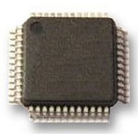
Manufacturer Part Number
DP83848VYB
Description
TRANSCEIVER, ENET PHY, 10/100, 48LQFP
Manufacturer
National Semiconductor
Datasheet
1.DP83848VYB.pdf
(76 pages)
Specifications of DP83848VYB
Data Rate
100Mbps
No. Of Ports
1
Ethernet Type
IEEE 802.3u
Supply Current
92mA
Supply Voltage Range
3V To 3.6V
Operating Temperature Range
-40°C To +105°C
Digital Ic Case Style
LQFP
No.
RoHS Compliant
Interface Type
MII Serial, RMII
Rohs Compliant
Yes
Lead Free Status / Rohs Status
Not Compliant
Available stocks
Company
Part Number
Manufacturer
Quantity
Price
Company:

Part Number:
DP83848VYB/NOPB
Manufacturer:
NS
Quantity:
570
Company:
Part Number:
DP83848VYB/NOPB
Manufacturer:
Texas Instruments
Quantity:
10 000


www.national.com
3.3 10 Mb SERIAL NETWORK INTERFACE (SNI)
The DP83848VYB incorporates a 10 Mb Serial Network In-
terface (SNI) which allows a simple serial data interface for
10 Mb only devices. This is also referred to as a 7-wire inter-
face. While there is no defined standard for this interface, it is
based on early 10 Mb physical layer devices. Data is clocked
serially at 10 MHz using separate transmit and receive paths.
The following pins are used in SNI mode:
— TX_CLK
— TX_EN
— TXD[0]
— RX_CLK
— RXD[0]
— CRS
— COL
3.4 802.3u MII SERIAL MANAGEMENT INTERFACE
3.4.1 Serial Management Register Access
The serial management MII specification defines a set of thir-
ty-two 16-bit status and control registers that are accessible
through the management interface pins MDC and MDIO. The
DP83848VYB implements all the required MII registers as
well as several optional registers. These registers are fully
described in 7.0 Register Block. A description of the serial
management access protocol follows.
3.4.2 Serial Management Access Protocol
The serial control interface consists of two pins, Management
Data Clock (MDC) and Management Data Input/Output
(MDIO). MDC has a maximum clock rate of 25 MHz and no
minimum rate. The MDIO line is bi-directional and may be
shared by up to 32 devices. The MDIO frame format is shown
below in Table 5.
The MDIO pin requires a pull-up resistor (1.5 kΩ) which, dur-
ing IDLE and turnaround, will pull MDIO high. In order to
Read Operation
Write Operation
Start Threshold RBR[1:0]
MII Management Serial Protocol
3 (12-bits)
0 (16-bits)
1 (4-bits)
2 (8-bits)
TABLE 4. Supported Packet Sizes at +/-50ppm +/-100ppm For Each Clock
Latency Tolerance
10 bits
14 bits
2 bits
6 bits
TABLE 5. Typical MDIO Frame Format
<idle><start><op code><device addr><reg addr><turnaround><data><idle>
<idle><01><10><AAAAA><RRRRR><Z0><xxxx xxxx xxxx xxxx><idle>
<idle><01><01><AAAAA><RRRRR><10><xxxx xxxx xxxx xxxx><idle>
Recommended Packet Size
18
at +/- 50ppm
12,000 bytes
16,800 bytes
initialize the MDIO interface, the station management entity
sends a sequence of 32 contiguous logic ones on MDIO to
provide the DP83848VYB with a sequence that can be used
to establish synchronization. This preamble may be generat-
ed either by driving MDIO high for 32 consecutive MDC clock
cycles, or by simply allowing the MDIO pull-up resistor to pull
the MDIO pin high during which time 32 MDC clock cycles are
provided. In addition 32 MDC clock cycles should be used to
re-sync the device if an invalid start, opcode, or turnaround
bit is detected.
The DP83848VYB waits until it has received this preamble
sequence before responding to any other transaction. Once
the DP83848VYB serial management port has been initial-
ized no further preamble sequencing is required until after a
power-on/reset, invalid Start, invalid Opcode, or invalid
turnaround bit has occurred.
The Start code is indicated by a <01> pattern. This assures
the MDIO line transitions from the default idle line state.
Turnaround is defined as an idle bit time inserted between the
Register Address field and the Data field. To avoid contention
during a read transaction, no device shall actively drive the
MDIO signal during the first bit of Turnaround. The addressed
DP83848VYB drives the MDIO with a zero for the second bit
of turnaround and follows this with the required data. Figure
3 shows the timing relationship between MDC and the MDIO
as
DP83848VYB (PHY) for a typical register read access.
For write transactions, the station management entity writes
data to the addressed DP83848VYB thus eliminating the re-
quirement for MDIO Turnaround. The Turnaround time is
filled by the management entity by inserting <10>. Figure 4
shows the timing relationship for a typical MII register write
access.
2,400 bytes
7,200 bytes
driven/received
by
Recommended Packet Size
the
at +/- 100ppm
Station
1,200 bytes
3,600 bytes
6,000 bytes
8,400 bytes
(STA)
and
the
Related parts for DP83848VYB
Image
Part Number
Description
Manufacturer
Datasheet
Request
R

Part Number:
Description:
National Semiconductor [8-Bit D/A Converter]
Manufacturer:
National Semiconductor
Datasheet:
Part Number:
Description:
National Semiconductor [Media Coprocessor]
Manufacturer:
National Semiconductor
Datasheet:
Part Number:
Description:
Digitally Controlled Tone and Volume Circuit with Stereo Audio Power Amplifier, Microphone Preamp Stage and National 3D Sound
Manufacturer:
National Semiconductor
Datasheet:
Part Number:
Description:
Digitally Controlled Tone and Volume Circuit with Stereo Audio Power Amplifier, Microphone Preamp Stage and National 3D Sound
Manufacturer:
National Semiconductor
Datasheet:
Part Number:
Description:
AC97 Rev 2 Codec with Sample Rate Conversion and National 3D Sound
Manufacturer:
National Semiconductor
Part Number:
Description:
Manufacturer:
National Semiconductor
Datasheet:
Part Number:
Description:
Manufacturer:
National Semiconductor
Datasheet:
Part Number:
Description:
General Purpose, Low Voltage, Low Power, Rail-to-Rail Output Operational Amplifiers
Manufacturer:
National Semiconductor
Datasheet:
Part Number:
Description:
8-bit 20 MSPS flash A/D converter.
Manufacturer:
National Semiconductor
Datasheet:
Part Number:
Description:
Low Noise Quad Operational Amplifier
Manufacturer:
National Semiconductor
Datasheet:
Part Number:
Description:
Quad Differential Line Receivers
Manufacturer:
National Semiconductor
Datasheet:
Part Number:
Description:
Quad High Speed Trapezoidal? Bus Transceiver
Manufacturer:
National Semiconductor
Datasheet:
Part Number:
Description:
Dual Line Receiver
Manufacturer:
National Semiconductor
Datasheet:
Part Number:
Description:
TTL to 10k ECL Level Translator with Latch
Manufacturer:
National Semiconductor
Datasheet: