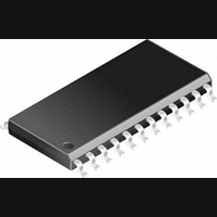
USBN9603-28M National Semiconductor, USBN9603-28M Datasheet - Page 19

USBN9603-28M
Manufacturer Part Number
USBN9603-28M
Description
USB Controller IC
Manufacturer
National Semiconductor
Specifications of USBN9603-28M
Interface
USB
No. Of Pins
28
Peak Reflow Compatible (260 C)
No
Supply Voltage Max
7V
Leaded Process Compatible
No
Controller Type, Ic
USB
Package / Case
28-WSOIC
Lead Free Status / RoHS Status
Contains lead / RoHS non-compliant
Available stocks
Company
Part Number
Manufacturer
Quantity
Price
Part Number:
USBN9603-28M
Manufacturer:
NS/国半
Quantity:
20 000
Company:
Part Number:
USBN9603-28M/NOPB
Manufacturer:
nsc
Quantity:
2 690
Company:
Part Number:
USBN9603-28MX
Manufacturer:
NSC
Quantity:
189
Part Number:
USBN9603-28MX
Manufacturer:
NS/国半
Quantity:
20 000
Company:
Part Number:
USBN9603-28MX/NOPB
Manufacturer:
NS
Quantity:
3 000
Part Number:
USBN9603-28MX/NOPB
Manufacturer:
NS/国半
Quantity:
20 000
5.0 MICROWIRE/PLUS Interface
The MICROWIRE/PLUS interface allows the USBN9603 to function as a CPU or microcontroller peripheral via a serial in-
terface. This mode is selected by pulling the MODE1 pin high and the MODE0 pin low. The MICROWIRE/PLUS mode uses
the chip select (CS), serial clock (SK), serial data in (SI) and serial data out (SO) pins, as shown in Figure 14.
5.1 OPERATING COMMANDS
The MICROWIRE/PLUS interface is enabled by a falling edge of CS and reset with a rising edge of CS. Data on SI is shifted
in after the rising edge of SK. Data is shifted out on SO after the falling edge of SK. Data is transferred from/to the Shift
register after the falling edge of the eighth SK clock. Data is transferred with the most significant bit first. Table 2 summarizes
the available commands (CMD) for the MICROWIRE/PLUS interface.
Note: A write operation to any register always reads the contents of the register after the write has occurred, and shifts out
that data in the next cycle. This read does not clear the bit in the respective registers, even for a Clear on Read (CoR) type
bit, with one exception: writing to the TXDx (transmit data) registers, which causes undefined data to be read during the next
cycle.
SK
CS
SO
SI
CMD
1 0 5
0 0
0 1
1 0
1 1
Byte Transferred
SYNC
(normal write)
4
(burst write)
1. 1 cycle = 8 SK clocks. Data is transferred after the 8th SK of 1 cycle.
WADDR
WADDR
RADDR
ADDR
(read)
3
x
2
Figure 14. MICROWIRE/PLUS Interface Block Diagram
1
0
CMD1-0
Table 2. Command/Address Byte Format
Cycle
2-n
1
2
1
1
2
1
DATA_IN
DATA_OUT
Shift in CMD/RADDR; shift out previous read data
Shift in next CMD/ADDR; shift out RADDR data
no action; shift out previous read data (do not clear CoR bits)
Shift in CMD/WADDR; shift out previous read data
Shift in WADDR write data; shift out WADDR read data (do
not clear CoR bits)
Shift in CMD/WADDR; shift out previous read data
Shift in WADDR write data; shift out WADDR read data (do
not clear CoR bits); terminate this mode by pulling CS high
SHIFT
ADDR
19
Sequence Initiated
Description
Data Out
Address
Data In
1
0x00
0x3F
Register File
www.national.com


