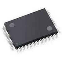
NJU6624CFG1-02 NJR, NJU6624CFG1-02 Datasheet - Page 10

NJU6624CFG1-02
Manufacturer Part Number
NJU6624CFG1-02
Description
LCD Drivers 14-Char/1-Line Dot Mtrx LCD Cntrlr Drvr
Manufacturer
NJR
Datasheet
1.NJU6624CFG1-02.pdf
(36 pages)
Specifications of NJU6624CFG1-02
Number Of Digits
14
Number Of Segments
70
Maximum Clock Frequency
218 KHz
Operating Supply Voltage
2.4 V to 5.5 V
Maximum Power Dissipation
500 mW
Maximum Operating Temperature
+ 85 C
Package / Case
QFP-100-G1
Maximum Supply Current
500 uA
Minimum Operating Temperature
- 40 C
Lead Free Status / RoHS Status
Lead free / RoHS Compliant
Available stocks
Company
Part Number
Manufacturer
Quantity
Price
Part Number:
NJU6624CFG1-02
Manufacturer:
JRC
Quantity:
20 000
(1-9)Keyscan circuit
(1-9)Keyscan circuit
-Request signal output
-Request signal output
When the NJU6624A/B detect the key-in by the key scan circuit, it outputs “H” signal as the request signal from
When the NJU6624A/B detect the key-in by the key scan circuit, it outputs “H” signal as the request signal from
the “REQ” terminal to notice the key pressing information to an application system.
the “REQ” terminal to notice the key pressing information to an application system.
The request signal resets to “L” level before 2 clock of next scanning.
The request signal resets to “L” level before 2 clock of next scanning.
-Contents of key register renewal
-Contents of key register renewal
Contents of key register are “0000 0000” in case of no key operation. Contents of key register are not changed in
Contents of key register are “0000 0000” in case of no key operation. Contents of key register are not changed in
busy of key data reading operation. Key data is fetched into the key register after 2 clock of the end of a keyscan
busy of key data reading operation. Key data is fetched into the key register after 2 clock of the end of a keyscan
cycle and kept by the start of next cycle.
cycle and kept by the start of next cycle.
-Key data input terminal and segment terminal
-Key data input terminal and segment terminal
Keyscan signal output terminals operate as segment terminals (SEG1 to SEG8) also and keyscan signals are
Keyscan signal output terminals operate as segment terminals (SEG1 to SEG8) also and keyscan signals are
output in interval period of segment signals. Key data input terminals (K0 to K3) are pulled up to VDD in busy of
output in interval period of segment signals. Key data input terminals (K0 to K3) are pulled up to VDD in busy of
keyscan operation (tKS). In this period, terminals of SEG9 to SEG71 output the voltage of V2 or V
keyscan operation (tKS). In this period, terminals of SEG9 to SEG71 output the voltage of V2 or V
-Keyscan OFF mode
-Keyscan OFF mode
Keyscan operation is turned ON or OFF by the instruction. In case of keyscan OFF, the detector of key pressing
Keyscan operation is turned ON or OFF by the instruction. In case of keyscan OFF, the detector of key pressing
is not operating and key data input terminals (K0 to K3) are not pulled up during the period of keyscan (tKS). In
is not operating and key data input terminals (K0 to K3) are not pulled up during the period of keyscan (tKS). In
the period of keyscan (tKS), all of segment terminals (SEG1 to SEG71) output the voltage of V2 or V
the period of keyscan (tKS), all of segment terminals (SEG1 to SEG71) output the voltage of V2 or V
-Example Keyscan
-Example Keyscan
SEG1/S0
SEG1/S0
SEG2/S1
SEG2/S1
SEG3/S2
SEG3/S2
SEG4/S3
SEG4/S3
SEG5/S4
SEG5/S4
SEG6/S5
SEG6/S5
SEG7/S6
SEG7/S6
SEG8/S7
SEG8/S7
The Keyscan circuit consists of a detector block of key pressing and a fetching block of key status. It scans 4x8
The Keyscan circuit consists of a detector block of key pressing and a fetching block of key status. It scans 4x8
key matrix and fetches conditions of 32 keys. Furthermore, it operates correctly against the key roll over input.
key matrix and fetches conditions of 32 keys. Furthermore, it operates correctly against the key roll over input.
REQ
REQ
S 0
S 1
S 2
S 3
S 4
S 5
S 6
S 7
tKS
tKS
S 0
S 1
S 2
S 3
S 4
S 5
S 6
S 7
NJU6624A/B
NJU6624A/B
S 0
S 1
S 2
S 3
S 4
S 5
S 6
S 7
LCD2
LCD2
LCD2
LCD2
. .
. .


