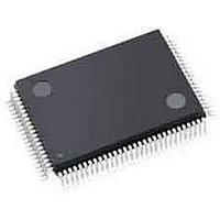
NJU6624CFG1-02 NJR, NJU6624CFG1-02 Datasheet - Page 27

NJU6624CFG1-02
Manufacturer Part Number
NJU6624CFG1-02
Description
LCD Drivers 14-Char/1-Line Dot Mtrx LCD Cntrlr Drvr
Manufacturer
NJR
Datasheet
1.NJU6624CFG1-02.pdf
(36 pages)
Specifications of NJU6624CFG1-02
Number Of Digits
14
Number Of Segments
70
Maximum Clock Frequency
218 KHz
Operating Supply Voltage
2.4 V to 5.5 V
Maximum Power Dissipation
500 mW
Maximum Operating Temperature
+ 85 C
Package / Case
QFP-100-G1
Maximum Supply Current
500 uA
Minimum Operating Temperature
- 40 C
Lead Free Status / RoHS Status
Lead free / RoHS Compliant
Available stocks
Company
Part Number
Manufacturer
Quantity
Price
Part Number:
NJU6624CFG1-02
Manufacturer:
JRC
Quantity:
20 000
( ( 5)LCD display
(5-1)Bleeder Resistance
(5-1)Bleeder Resistance
(5-2)Relation between oscillation frequency and LCD frame frequency
(5-2)Relation between oscillation frequency and LCD frame frequency
5)LCD display
Each LCD driving voltage ( V
Each LCD driving voltage ( V
the E.V.R. and high impedance bleeder resistance.
the E.V.R. and high impedance bleeder resistance.
The bleeder resistance is set 1/4 bias suitable for 1/8 duty ratio.
The bleeder resistance is set 1/4 bias suitable for 1/8 duty ratio.
The capacitor connected between VLCD2 and V
The capacitor connected between VLCD2 and V
capacitance requires to operate with the LCD panel actually.
capacitance requires to operate with the LCD panel actually.
As the NJU6624A/B incorporate oscillation capacitor and resistor for CR oscillation, 145kHz oscillation is avail-
As the NJU6624A/B incorporate oscillation capacitor and resistor for CR oscillation, 145kHz oscillation is avail-
able without any external components.
able without any external components.
The LCD frame frequency example mentioned below is based on 145kHz oscillation.(1clock =6.90us)
The LCD frame frequency example mentioned below is based on 145kHz oscillation.(1clock =6.90us)
COM1
COM1
VLCD
VLCD
VSS
VSS
V4
V4
V1
V1
V2
V2
VLCD2
VLCD2
VLCD1
VLCD1
VSS
VSS
V1
V1
V2
V2
V4
V4
2 2 4 c l o c k s
I c o n
1 frame = 6.90(us) x 224 x 8 = 12.36(ms)
1 frame = 6.90(us) x 224 x 8 = 12.36(ms)
Frame frequency = 1 / 12.36(ms) = 79.50(Hz)
Frame frequency = 1 / 12.36(ms) = 79.50(Hz)
Key scan time = 220.70(uS)
Key scan time = 220.70(uS)
V V
1
LCD
LCD
P o w e r
s u p p l y
1 1
+
, V
, V
2
is the maximum amplitude for LCD driving voltage.
is the maximum amplitude for LCD driving voltage.
2 2
, V
, V
+
LCD Driving Voltage vs Duty Ratio
LCD Driving Voltage vs Duty Ratio
3
1 f r a m e
V
3 3
, V
, V
+
Duty Ratio
LCD
4 4
..............
Bias
+
) is
) is LCD driving high voltage input to the VLCD1 terminal,
LCD driving high voltage input to the VLCD1 terminal, generated by
SS
SS
7
is needed for stabilizing VLCD. The determination of the each
is needed for stabilizing VLCD. The determination of the each
6.6 K
4K
4K
4K
4K
4K
4K
4K
4K
E.V.R.(16Step)
E.V.R.(16Step)
K e y
Internal NJU6624
Internal NJU6624
I c o n
V L C D 2 - V S S
1/8
1/4
1
2
VLCD
VLCD
V2
V2 (V3)
VSS
VSS
V4
V4
V1
V1
3
1 f r a m e
(V3)
..............
NJU6624A/B
NJU6624A/B
VLCD
VLCD
7
K e y
generated by
I c o n
1
2


