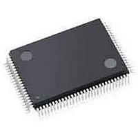
NJU6624CFG1-02 NJR, NJU6624CFG1-02 Datasheet - Page 24

NJU6624CFG1-02
Manufacturer Part Number
NJU6624CFG1-02
Description
LCD Drivers 14-Char/1-Line Dot Mtrx LCD Cntrlr Drvr
Manufacturer
NJR
Datasheet
1.NJU6624CFG1-02.pdf
(36 pages)
Specifications of NJU6624CFG1-02
Number Of Digits
14
Number Of Segments
70
Maximum Clock Frequency
218 KHz
Operating Supply Voltage
2.4 V to 5.5 V
Maximum Power Dissipation
500 mW
Maximum Operating Temperature
+ 85 C
Package / Case
QFP-100-G1
Maximum Supply Current
500 uA
Minimum Operating Temperature
- 40 C
Lead Free Status / RoHS Status
Lead free / RoHS Compliant
Available stocks
Company
Part Number
Manufacturer
Quantity
Price
Part Number:
NJU6624CFG1-02
Manufacturer:
JRC
Quantity:
20 000
(k)Set Display Mode
(k)Set Display Mode
(j)Set DD/MK RAM Address
(j)Set DD/MK RAM Address
(j)Set CG RAM Address
(j)Set CG RAM Address
The key scan operation when switching to the power down mode during key scan.
The key scan operation when switching to the power down mode during key scan.
When switching to the power down mode during key scan operation, it stops key scan operation
When switching to the power down mode during key scan operation, it stops key scan operation
in the period and after power down mode cancellation too.
in the period and after power down mode cancellation too.
before switches to power down mode and REQ signal rises to"H".
before switches to power down mode and REQ signal rises to"H".
However, the key scan operation becomes invalid data even if it reads key-in data because
However, the key scan operation becomes invalid data even if it reads key-in data because
it stoppd.The key data becomes to valid with the key scan by the next key scan of frame.
it stoppd.The key data becomes to valid with the key scan by the next key scan of frame.
The Set Display Mode instruction control the function of key scan and power down mode.
The Set Display Mode instruction control the function of key scan and power down mode.
In busy of Power down mode, do not input any instructions except for release the power down mode.
In busy of Power down mode, do not input any instructions except for release the power down mode.
The power down mode should be set before power off because any irregular display appearance at power off is
The power down mode should be set before power off because any irregular display appearance at power off is
prevented.
prevented.
After power down mode cancellation, the REQ signal maintains "H" when detects key-in signal
After power down mode cancellation, the REQ signal maintains "H" when detects key-in signal
The address data (DB
The address data (DB
After this instruction execution, the data writing is performed into the addressed
After this instruction execution, the data writing is performed into the addressed DD/MK
The RAM includes DD RAM and MK RAM, and these RAMs are shared by address as shown below.
The RAM includes DD RAM and MK RAM, and these RAMs are shared by address as shown below.
The CG RAM address set instruction is executed when the "H" level input to the AC terminal and the address is
The CG RAM address set instruction is executed when the "H" level input to the AC terminal and the address is
written into DB
written into DB
The address data (DB
The address data (DB
After this instruction execution, the data writing is performed into the addressed RAM.
After this instruction execution, the data writing is performed into the addressed RAM.
The RAM includes CG RAM address as shown below.
The RAM includes CG RAM address as shown below.
Code
Code
Code
7 7
PD
to DB
to DB
K
0
0
1
1
D15 D14 D13 D12 D11 D10 D9
D15 D14 D13 D12 D11 D10 D9
D15 D14 D13 D12 D11 D10 D9
MS1 MS0
MS1 MS0
MS1 MS0
4 4
0 0
7 7
to DB
to DB
as shown above.
as shown above.
to DB
to DB
Key scan ON
Key scan OFF
In busy of keyscan (tKS), all of segment terminal (S0 to S7) output the voltage
of V2.or V
Power down mode. All of common and segment terminal set the voltage level
of VLCD2
Release the power down mode.
0 0
0 0
) is written into the address counter (AC) by this instruction.
) is written into the address counter (AC) by this instruction.
) is written into the address counter (AC) by this instruction.
) is written into the address counter (AC) by this instruction.
0
0
0
LCD2
DD RAM
DD RAM
MK RAM
MK RAM
CG RAM
CG RAM
0
1
1
0
0
1
: :
: :
: :
0
0
1
RAM address
RAM address
(00)
(00)
(10)
(10)
RAM address
RAM address
(00)
(00)
0
1
1
F u n c t i o n
F u n c t i o n
H H
H H
H H
D8
D8
D8
- (0D)
- (0D)
- (1D)
- (1D)
- (FE)
- (FE)
0
0
1
AC7 AC6 AC5 AC4 AC3 AC2 AC1 AC0
D7
D7
D7
H H
H H
H H
*
*
D6
D6
D6
*
*
D5
D5
D5
*
*
DD/MK RAM.
NJU6624A/B
NJU6624A/B
AD4 AD3 AD2 AD1 AD0
D4
D4
D4
*
RAM.
D3
D3
D3
*
D2
D2
D2
*
D1
D1
D1
K
PD
D0
D0
D0


