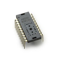
ADNS-6010 Avago Technologies US Inc., ADNS-6010 Datasheet - Page 17

ADNS-6010
Manufacturer Part Number
ADNS-6010
Description
Optical Sensors - Board Mount Laser mouse sensor
Manufacturer
Avago Technologies US Inc.
Datasheet
1.ADNS-6010.pdf
(41 pages)
Specifications of ADNS-6010
Lead Free Status / RoHS Status
Lead free / RoHS Compliant
Available stocks
Company
Part Number
Manufacturer
Quantity
Price
Required timing between Read and Write Commands
(tsxx)
There are minimum timing requirements between read
and write commands on the serial port.
Figure 19. MISO Delay and Hold Time
If the rising edge of the SCLK for the last data bit of the
second write command occurs before the 50 microsec-
ond required delay, then the first write command may
not complete correctly.
If the rising edge of SCLK for the last address bit of
the read command occurs before the 50 microsecond
required delay, the write command may not complete
correctly.
Figure 20. Timing between two write commands
SCLK
Figure 21. Timing between write and read commands
Figure 22. Timing between read and either write or subsequent read commands
17
t
SCLK
SCLK
DLY-MISO
SCLK
MISO
Address
Address
Address
D
0
Write Operation
Write Operation
t
HOLD-MISO
≥ t
Data
Data
t
SRAD
SRAD MOT
75 μs for register 0x02
50 μs for non-motion read
Read Operation
Address
The falling edge of SCLK for the first address bit of either
the read or write command must be at least 250 ns after
the last SCLK rising edge of the last data bit of the previ-
ous read operation. In addition, during a read operation
SCLK should be delayed after the last address data bit
to ensure that the ADNS-6010 has time to prepare the
requested data.
Burst Mode Operation
Burst mode is a special serial port operation mode which
may be used to reduce the serial transaction time for
three predefined operations: motion read and PROM
download and frame capture. The speed improvement is
achieved by continuous data clocking to or from multiple
registers without the need to specify the register address,
and by not requiring the normal delay period between
data bytes.
≥ t
≥ t
SWW
SWR
Write Operation
50 μ s
50 μ s
Data
Address
Next Read
Operation
Data
t
SRW
& t
SRR
>250 ns
Write Operation
Next Read or
Address


