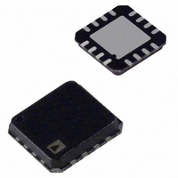
ADA4927-1YCPZ-R7 Analog Devices Inc, ADA4927-1YCPZ-R7 Datasheet - Page 16

ADA4927-1YCPZ-R7
Manufacturer Part Number
ADA4927-1YCPZ-R7
Description
UltraLw Distortion Crnt Fdbck ADC Driver
Manufacturer
Analog Devices Inc
Datasheet
1.ADA4927-2YCPZ-R2.pdf
(24 pages)
Specifications of ADA4927-1YCPZ-R7
Amplifier Type
Current Feedback
Number Of Circuits
1
Output Type
Differential
Slew Rate
5000 V/µs
-3db Bandwidth
2.3GHz
Current - Input Bias
500nA
Voltage - Input Offset
300µV
Current - Supply
20mA
Current - Output / Channel
65mA
Voltage - Supply, Single/dual (±)
4.5 V ~ 11 V, ±2.25 V ~ 5.5 V
Operating Temperature
-40°C ~ 105°C
Mounting Type
Surface Mount
Package / Case
16-LFCSP
Lead Free Status / RoHS Status
Lead free / RoHS Compliant
Gain Bandwidth Product
-
Lead Free Status / RoHS Status
Lead free / RoHS Compliant
Other names
ADA4927-1YCPZ-R7TR
Available stocks
Company
Part Number
Manufacturer
Quantity
Price
Company:
Part Number:
ADA4927-1YCPZ-R7
Manufacturer:
Cortina
Quantity:
5
ADA4927-1/ADA4927-2
THEORY OF OPERATION
The ADA4927 differs from conventional operational amplifiers
in that it has two outputs whose voltages move in opposite
directions and an additional input, V
uses a current feedback architecture. Like a traditional current
feedback op amp, the ADA4927 relies on high open-loop trans-
impedance, T(s), and negative current feedback to force the
outputs to the desired voltages. The ADA4927 behaves much
like a standard current feedback op amp and facilitates single-
ended-to-differential conversions, common-mode level shifting,
and amplifications of differential signals. Also, like a current
feedback op amp, the ADA4927 has low input impedance
summing nodes, which are actually emitter-follower outputs.
The ADA4927 outputs are low impedance, and the closed-loop
output impedances are equal to the open-loop output impedances
divided by a factor of 1 + loop gain. Because it uses current
feedback, the ADA4927 manifests a nominally constant feed-
back resistance, bandwidth product. In other words, the closed-
loop bandwidth and stability of the ADA4927 depend primarily
on the feedback resistor value. The closed-loop gain equations
for typical configurations are the same as those of comparable
voltage feedback differential amplifiers. The chief difference is
that the ADA4927 dynamic performance depends on the feed-
back resistor value rather than on the noise gain. Because of
this, the elements used in the feedback loops must be resistive
with values that ensure stability and sufficient bandwidth.
Two feedback loops are employed to control the differential and
common-mode output voltages. The differential feedback loops
use a current feedback architecture with external resistors and
control only the differential output voltage. The common-mode
feedback loop is internal, uses voltage feedback, and controls only
the common-mode output voltage. This architecture makes it
easy to set the output common-mode level to any arbitrary
value within the specified limits. The output common-mode
voltage is forced, by the internal common-mode loop, to be
equal to the voltage applied to the V
The internal common-mode feedback loop produces outputs
that are highly balanced over a wide frequency range without
requiring tightly matched external components. This results
in differential outputs that are very close to the ideal of being
identical in amplitude and are exactly 180° apart in phase.
OCM
OCM
. Moreover, the ADA4927
input.
Rev. A | Page 16 of 24
DEFINITION OF TERMS
Differential Voltage
Differential voltage refers to the difference between two
node voltages. For example, the output differential voltage (or
equivalently, output differential-mode voltage) is defined as
where V
−OUT terminals with respect to a common ground reference.
Similarly, the differential input voltage is defined as
Common-Mode Voltage
Common-mode voltage refers to the average of two node voltages
with respect to the local ground reference. The output
common-mode voltage is defined as
Balance
Output balance is a measure of how close the differential signals
are to being equal in amplitude and opposite in phase. Output
balance is most easily determined by placing a well-matched
resistor divider between the differential voltage nodes and
comparing the magnitude of the signal at the divider midpoint
with the magnitude of the differential signal (see Figure 44). By
this definition, output balance is the magnitude of the output
common-mode voltage divided by the magnitude of the output
differential mode voltage.
V
V
V
Output
V
+D
–D
OUT, dm
IN, dm
OUT, cm
OCM
+FB
–FB
+OUT
IN
IN
= (+D
= (V
= (V
and V
Balance
R
R
G
G
R
+OUT
R
+OUT
IN
F
F
−OUT
− (−D
Figure 46. Circuit Definitions
+IN
+ V
–IN
− V
Error
refer to the voltages at the +OUT and
−OUT
−OUT
IN
ADA4927
))
=
)/2
)
Δ
Δ
V
V
OUT
OUT
–OUT
+OUT
,
,
dm
cm
R
L, dm
V
OUT, dm


