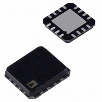
ADA4927-1YCPZ-R7 Analog Devices Inc, ADA4927-1YCPZ-R7 Datasheet - Page 8

ADA4927-1YCPZ-R7
Manufacturer Part Number
ADA4927-1YCPZ-R7
Description
UltraLw Distortion Crnt Fdbck ADC Driver
Manufacturer
Analog Devices Inc
Datasheet
1.ADA4927-2YCPZ-R2.pdf
(24 pages)
Specifications of ADA4927-1YCPZ-R7
Amplifier Type
Current Feedback
Number Of Circuits
1
Output Type
Differential
Slew Rate
5000 V/µs
-3db Bandwidth
2.3GHz
Current - Input Bias
500nA
Voltage - Input Offset
300µV
Current - Supply
20mA
Current - Output / Channel
65mA
Voltage - Supply, Single/dual (±)
4.5 V ~ 11 V, ±2.25 V ~ 5.5 V
Operating Temperature
-40°C ~ 105°C
Mounting Type
Surface Mount
Package / Case
16-LFCSP
Lead Free Status / RoHS Status
Lead free / RoHS Compliant
Gain Bandwidth Product
-
Lead Free Status / RoHS Status
Lead free / RoHS Compliant
Other names
ADA4927-1YCPZ-R7TR
Available stocks
Company
Part Number
Manufacturer
Quantity
Price
Company:
Part Number:
ADA4927-1YCPZ-R7
Manufacturer:
Cortina
Quantity:
5
ADA4927-1/ADA4927-2
PIN CONFIGURATIONS AND FUNCTION DESCRIPTIONS
Table 9. ADA4927-1 Pin Function Descriptions
Pin No.
1
2
3
4
5 to 8
9
10
11
12
13 to 16
17 (EPAD)
+FB
NOTES
1. CONNECT THE EXPOSED PADDLE TO ANY PLANE
–FB
+IN
–IN
BETWEEN AND INCLUDING +V
Mnemonic
−FB
+IN
−IN
+FB
+V
V
+OUT
−OUT
PD
−V
Exposed
Pad (EPAD)
OCM
1
2
3
4
S
S
Figure 5. ADA4927-1 Pin Configuration
ADA4927-1
(Not to Scale)
TOP VIEW
PIN 1
INDICATOR
Description
Negative Output for Feedback
Component Connection
Positive Input Summing Node
Negative Input Summing Node
Positive Output for Feedback
Component Connection
Positive Supply Voltage
Output Common-Mode Voltage
Positive Output for Load Connection
Negative Output for Load Connection
Power-Down Pin
Negative Supply Voltage
Connect the exposed pad to any
plane between and including
+V
S
12 PD
11 –OUT
10 +OUT
9 V
and −V
S
OCM
AND –V
S
.
S
.
Rev. A | Page 8 of 24
Table 10. ADA4927-2 Pin Function Descriptions
Pin No.
1
2
3, 4
5
6
7
8
9, 10
11
12
13
14
15, 16
17
18
19
20
21, 22
23
24
25 (EPAD)
+FB1
–FB2
NOTES
1. CONNECT THE EXPOSED PADDLE TO ANY PLANE
+V
+V
–IN1
+IN2
BETWEEN AND INCLUDING +V
S1
S1
Mnemonic
−IN1
+FB1
+V
−FB2
+IN2
−IN2
+FB2
+V
V
+OUT2
−OUT2
PD2
−V
V
+OUT1
−OUT1
PD1
−V
−FB1
+IN1
Exposed
Pad (EPAD)
OCM2
OCM1
1
2
3
4
5
6
S1
S2
S2
S1
Figure 6. ADA4927-2 Pin Configuration
ADA4927-2
(Not to Scale)
TOP VIEW
PIN 1
INDICATOR
Description
Negative Input Summing Node 1
Positive Output Feedback 1
Positive Supply Voltage 1
Negative Output Feedback 2
Positive Input Summing Node 2
Negative Input Summing Node 2
Positive Output Feedback 2
Positive Supply Voltage 2
Output Common-Mode Voltage 2
Positive Output 2
Negative Output 2
Power-Down Pin 2
Negative Supply Voltage 2
Output Common-Mode Voltage 1
Positive Output 1
Negative Output 1
Power-Down Pin 1
Negative Supply Voltage 1
Negative Output Feedback 1
Positive Input Summing Node 1
Connect the exposed pad to any
plane between and including
+V
S
and −V
18
17
16
15
14
13
S
+OUT1
V
–V
–V
PD2
–OUT2
AND –V
OCM1
S2
S2
S
.
S
.


