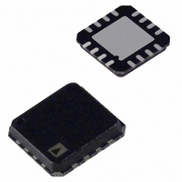
ADA4927-1YCPZ-R7 Analog Devices Inc, ADA4927-1YCPZ-R7 Datasheet - Page 18

ADA4927-1YCPZ-R7
Manufacturer Part Number
ADA4927-1YCPZ-R7
Description
UltraLw Distortion Crnt Fdbck ADC Driver
Manufacturer
Analog Devices Inc
Datasheet
1.ADA4927-2YCPZ-R2.pdf
(24 pages)
Specifications of ADA4927-1YCPZ-R7
Amplifier Type
Current Feedback
Number Of Circuits
1
Output Type
Differential
Slew Rate
5000 V/µs
-3db Bandwidth
2.3GHz
Current - Input Bias
500nA
Voltage - Input Offset
300µV
Current - Supply
20mA
Current - Output / Channel
65mA
Voltage - Supply, Single/dual (±)
4.5 V ~ 11 V, ±2.25 V ~ 5.5 V
Operating Temperature
-40°C ~ 105°C
Mounting Type
Surface Mount
Package / Case
16-LFCSP
Lead Free Status / RoHS Status
Lead free / RoHS Compliant
Gain Bandwidth Product
-
Lead Free Status / RoHS Status
Lead free / RoHS Compliant
Other names
ADA4927-1YCPZ-R7TR
Available stocks
Company
Part Number
Manufacturer
Quantity
Price
Company:
Part Number:
ADA4927-1YCPZ-R7
Manufacturer:
Cortina
Quantity:
5
ADA4927-1/ADA4927-2
Table 12. Differential Input, DC-Coupled
Nominal Gain (dB)
0
20
26
Table 13. Single-Ended Ground-Referenced Input, DC-Coupled, R
Nominal Gain (dB)
0
20
26
1
Similar to the case of a conventional op amp, the output noise
voltage densities can be estimated by multiplying the input-
referred terms at +IN and −IN by the appropriate output factor,
where:
When the feedback factors are matched, R
β1 = β2 = β, and the noise gain becomes
Note that the output noise from V
The total differential output noise density, v
square of the individual output noise terms.
Table 12 and Table 13 list several common gain settings, associated
resistor values, input impedance, and output noise density for
both balanced and unbalanced input configurations.
IMPACT OF MISMATCHES IN THE FEEDBACK
NETWORKS
As previously mentioned, even if the external feedback networks
(R
loop still forces the outputs to remain balanced. The amplitudes
of the signals at each output remain equal and 180° out of phase.
The input-to-output differential mode gain varies proportionately
to the feedback mismatch, but the output balance is unaffected.
The gain from the V
When β1 = β2, this term goes to zero and there is no differential
output voltage due to the voltage on the V
noise). The extreme case occurs when one loop is open and the
other has 100% feedback; in this case, the gain from V
to V
G
β
R
1
G2
N
F
=
/R
= R
=
O, dm
2(β1 − β2)/(β1 + β2)
G
v
R
G
(
nOD
G1
) are mismatched, the internal common-mode feedback
F1
N
β
R
is either +2 or −2, depending on which loop is closed.
1
+ (R
=
+
G1
+
2
=
R
1
β
S
β
||R
G1
2
=
∑
)
i
T
=
8
).
1
1
and
is the circuit noise gain.
v
+
nOi
2
R
R
G
F
β
OCM
2
=
pin to V
R
R
309
511
806
F2
F
R
(Ω)
+
G2
R
301
442
604
R
F
G2
O, dm
(Ω)
OCM
are the feedback factors.
R
301
39.2
28
is equal to
G1
goes to zero in this case.
(Ω)
OCM
F1
R
301
44.2
30.1
/R
nOD
G
input (including
G1
(Ω)
R
56.2
158
649
, is the root-sum-
T
= R
(Ω)
F2
/R
OCM
R
401
73.2
54.2
G2
R
602
88.4
60.2
IN, cm
IN, dm
,
input
Rev. A | Page 18 of 24
(Ω)
(Ω)
R
328
77.2
74.4
S
G2
= 50 Ω
(Ω)
Differential Output Noise Density (nV/√Hz)
8.0
21.8
37.9
The feedback loops are nominally matched to within 1% in
most applications, and the output noise and offsets due to the
V
by a large amount, it is necessary to include the gain term from
V
β1 = 0.5 and β2 = 0.25, the gain from V
V
output of (2.5 V)(0.67) = 1.67 V. The differential output noise
contribution is (15 nV/√Hz)(0.67) = 10 nV/√Hz. Both of these
results are undesirable in most applications; therefore, it is best
to use nominally matched feedback factors.
Mismatched feedback networks also result in a degradation of
the ability of the circuit to reject input common-mode signals,
much the same as for a four-resistor difference amplifier made
from a conventional op amp.
As a practical summarization of the previous issues, resistors of
1% tolerance produce a worst-case input CMRR of approximately
40 dB, a worst-case differential-mode output offset of 25 mV
due to a 2.5 V V
and no significant degradation in output balance error.
CALCULATING THE INPUT IMPEDANCE FOR AN
APPLICATION CIRCUIT
The effective input impedance of a circuit depends on whether
the amplifier is being driven by a single-ended or differential
signal source. For balanced differential input signals, as shown
in Figure 48, the input impedance (R
(+D
OCM
OCM
OCM
1
Figure 48. The ADA4927 Configured for Balanced (Differential) Inputs
IN
input are negligible. If the loops are intentionally mismatched
to V
pin is set to 2.5 V, a differential offset voltage is present at the
and −D
Differential Output Noise Density (nV/√Hz)
8.1
18.6
29.1
O, dm
+D
–D
IN
IN
IN
and account for the extra noise. For example, if
) is simply R
OCM
R
R
input, negligible V
G
G
V
OCM
+IN
–IN
IN, dm
ADA4927
+V
–V
R
R
S
= R
F
S
F
G
IN, dm
OCM
+ R
OCM
) between the inputs
to V
G
noise contribution,
= 2 × R
V
OUT, dm
O, dm
is 0.67. If the
G
.


