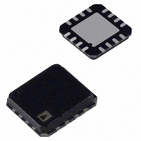
ADA4927-1YCPZ-R7 Analog Devices Inc, ADA4927-1YCPZ-R7 Datasheet - Page 3

ADA4927-1YCPZ-R7
Manufacturer Part Number
ADA4927-1YCPZ-R7
Description
UltraLw Distortion Crnt Fdbck ADC Driver
Manufacturer
Analog Devices Inc
Datasheet
1.ADA4927-2YCPZ-R2.pdf
(24 pages)
Specifications of ADA4927-1YCPZ-R7
Amplifier Type
Current Feedback
Number Of Circuits
1
Output Type
Differential
Slew Rate
5000 V/µs
-3db Bandwidth
2.3GHz
Current - Input Bias
500nA
Voltage - Input Offset
300µV
Current - Supply
20mA
Current - Output / Channel
65mA
Voltage - Supply, Single/dual (±)
4.5 V ~ 11 V, ±2.25 V ~ 5.5 V
Operating Temperature
-40°C ~ 105°C
Mounting Type
Surface Mount
Package / Case
16-LFCSP
Lead Free Status / RoHS Status
Lead free / RoHS Compliant
Gain Bandwidth Product
-
Lead Free Status / RoHS Status
Lead free / RoHS Compliant
Other names
ADA4927-1YCPZ-R7TR
Available stocks
Company
Part Number
Manufacturer
Quantity
Price
Company:
Part Number:
ADA4927-1YCPZ-R7
Manufacturer:
Cortina
Quantity:
5
SPECIFICATIONS
±5 V OPERATION
T
All specifications refer to single-ended input and differential outputs, unless otherwise noted. Refer to Figure 46 for signal definitions.
±D
Table 1.
Parameter
DYNAMIC PERFORMANCE
NOISE/HARMONIC PERFORMANCE
INPUT CHARACTERISTICS
OUTPUT CHARACTERISTICS
A
Second Harmonic
Third Harmonic
IMD
Voltage Noise (RTI)
Input Current Noise
Crosstalk
Offset Voltage
Input Bias Current
Input Offset Current
Input Resistance
Input Capacitance
Input Common-Mode Voltage Range
CMRR
Open-Loop Transresistance
Output Voltage Swing
Linear Output Current
Output Balance Error
−3 dB Small Signal Bandwidth
−3 dB Large Signal Bandwidth
Bandwidth for 0.1 dB Flatness
Slew Rate
Settling Time to 0.1%
Overdrive Recovery Time
= 25°C, +V
IN
to V
OUT, dm
S
= 5 V, −V
Performance
S
= − 5 V, V
OCM
= 0 V, R
Conditions
V
V
V
V
V
V
V
See Figure 45 for distortion test circuit
V
V
V
V
V
V
f
f
f = 100 kHz, G = 28
f = 100 kHz, G = 28
f = 100 MHz, ADA4927-2
V
t
t
Differential
Common mode
Differential
∆V
DC
Each single-ended output, R
∆V
see Figure 44 for test circuit
1
1
MIN
MIN
F
OUT, dm
OUT, dm
OUT, dm
OUT, dm
OUT, dm
OUT, dm
IN
OUT, dm
OUT, dm
OUT, dm
OUT, dm
OUT, dm
OUT, dm
IP
= 70 MHz, f
= 140 MHz, f
= 301 Ω, R
OUT, dm
OUT, cm
= V
= 0 V to 0.9 V step, G = 10
to t
to t
IN
= 0.1 V p-p
= 2.0 V p-p
= 0.1 V p-p, ADA4927-1
= 0.1 V p-p, ADA4927-2
= 2 V step, 25% to 75%
= 2 V step
= 2 V p-p, 10 MHz
= 2 V p-p, 70 MHz
= 2 V p-p, 100 MHz
= 2 V p-p, 10 MHz
= 2 V p-p, 70 MHz
= 2 V p-p, 100 MHz
MAX
MAX
/∆V
= V
/∆V
variation
variation
OCM
OUT, dm
IN, cm
2
G
Rev. A | Page 3 of 24
= 70.1 MHz, V
2
= 0 V
= 301 Ω, R
, ∆V
= 140.1 MHz, V
, ∆V
IN, cm
OUT, dm
= ±1 V
T
= 1 V, 10 MHz,
= 56.2 Ω (when used), R
OUT, dm
F
= R
OUT, dm
G
= 2 V p-p
= 10 kΩ
= 2 V p-p
L, dm
Min
−1.3
−15
−10.5
−3.5
−70
120
−3.8
ADA4927-1/ADA4927-2
= 1 kΩ, unless otherwise noted.
Typ
2300
1500
150
120
5000
10
10
−105
−91
−87
−103
−98
−89
−94
−85
1.4
14
−75
+0.3
±1.5
+0.5
±0.1
−0.6
14
120
0.5
−93
185
65
−65
Max
+1.3
+15
+10.5
+3.5
+3.8
Unit
MHz
MHz
V/μs
dBc
nV/√Hz
pA/√Hz
mV
μV/°C
μA/°C
kΩ
pF
dB
kΩ
MHz
MHz
ns
ns
dBc
dBc
dBc
dBc
dBc
dBc
dBc
dB
μA
μA
Ω
V
V
mA p-p
dB


