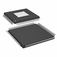
ADAU1445YSVZ-3A-RL Analog Devices Inc, ADAU1445YSVZ-3A-RL Datasheet - Page 44

ADAU1445YSVZ-3A-RL
Manufacturer Part Number
ADAU1445YSVZ-3A-RL
Description
175MHZ SigmaDSP,2x8 SRCs
Manufacturer
Analog Devices Inc
Series
SigmaDSP®r
Type
Audio Processorr
Specifications of ADAU1445YSVZ-3A-RL
Applications
Automotive Audio
Mounting Type
Surface Mount
Package / Case
100-TQFP Exposed Pad, 100-eTQFP, 100-HTQFP, 100-VQFP
Format
Fixed Point
Program Memory Size
Not RequiredKB
Operating Supply Voltage (typ)
1.8/3.3V
Operating Temp Range
-40C to 105C
Operating Temperature Classification
Industrial
Mounting
Surface Mount
Pin Count
100
Lead Free Status / RoHS Status
Lead free / RoHS Compliant
Lead Free Status / RoHS Status
Lead free / RoHS Compliant
Available stocks
Company
Part Number
Manufacturer
Quantity
Price
Company:
Part Number:
ADAU1445YSVZ-3A-RL
Manufacturer:
Analog Devices Inc
Quantity:
10 000
ADAU1445/ADAU1446
FLEXIBLE AUDIO ROUTING MATRIX (FARM)
The routing matrix distributes audio signals among the serial
inputs, serial outputs, ASRCs, S/PDIF receiver and transmitter,
and DSP core. This simplifies the design of complex systems
that require many inputs and outputs with different sample
rates. It also allows signals to be routed in hardware, instead of
in software.
Routing Matrix Block Diagram
Figure 36 shows an overview of audio routing in the ADAU1445/
ADAU1446 and details the interaction among the S/PDIF I/O,
serial I/O, ASRCs, and DSP via the routing matrix. To reduce
the complexity of the system, audio signals are routed in pairs.
Therefore, in Figure 36, each solid line represents a stereo pair
of audio signals. The corresponding channel numbers are
written above the lines. The dotted lines at the bottom of the
SDATA_IN0
SDATA_IN1
SDATA_IN2
SDATA_IN3
SDATA_IN4
SDATA_IN5
SDATA_IN6
SDATA_IN7
SDATA_IN8
SPDIFI
SERIAL
MODES
SERIAL
S
PORTS
P
INPUT
INPUT
(×9)
S
L
CHANNELS
S/PDIF Rx
(24 CH)
INPUT
10, 11
12, 13
14, 15
16, 17
18, 19
20, 21
22, 23
0, 1
2, 3
4, 5
6, 7
8, 9
MASTER/SLAVE
SELECT
Figure 36. Routing Matrix Block Diagram
10, 11
12, 13
14, 15
16, 17
18, 19
20, 21
22, 23
2
0 TO 2
0, 1
2, 3
4, 5
6, 7
8, 9
10, 11
12, 13
14, 15
0, 1
2, 3
4, 5
6, 7
8, 9
2
6
Rev. A | Page 44 of 92
10, 11
12, 13
14, 15
0, 1
2, 3
4, 5
6, 7
8, 9
2
CLOCK DOMAINS (×12)
2
SERIAL I/O
DSP CORE
2
S/PDIF I/O
(8 × 2 CH)
ASRC I/O
STEREO
(24 CH)
(16 CH)
ASRCS
(2 CH)
3 TO 8
2
12
2
2
diagram represent clock signals. The two large gray boxes represent
the flexible audio routing matrix, in which one-to-one connections
can be made between any input and any output. The signal routing
is fully implemented in hardware.
System Delay
Routing data through the serial ports, routing matrix, ASRCs,
and DSP core results in a brief delay between the time when an
audio sample is input to the IC and when it is output. If the DSP
is programmed to simply pass serial inputs to serial outputs with
no sample rate conversion or additional processing, the minimum
observed delay of an audio sample from the SDATA_INx pin to
the SDATA_OUTx pin is equal to four sample periods. At a sample
rate of 48 kHz, this corresponds to 83 μs. The system delay increases
as sample rate conversion or additional processing is implemented
in the system.
2
10, 11
12, 13
14, 15
0, 1
2, 3
4, 5
6, 7
8, 9
8
2
10, 11
12, 13
14, 15
9 TO 11
0, 1
2, 3
4, 5
6, 7
8, 9
10, 11
12, 13
14, 15
16, 17
18, 19
20, 21
22, 23
0, 1
2, 3
4, 5
6, 7
8, 9
RATE
2
6
2
10, 11
12, 13
14, 15
16, 17
18, 19
20, 21
22, 23
0, 1
2, 3
4, 5
6, 7
8, 9
S/PDIF Tx
CHANNELS
OUTPUT
(24 CH)
OUTPUT
SERIAL
MODES
OUTPUT
SERIAL
PORTS
(×9)
S/PDIF OUTPUT
ON MP PINS
SPDIFO
SDATA_OUT0
SDATA_OUT1
SDATA_OUT2
SDATA_OUT3
SDATA_OUT4
SDATA_OUT5
SDATA_OUT6
SDATA_OUT7
SDATA_OUT8


