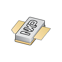
BLF6G22LS-100 NXP Semiconductors, BLF6G22LS-100 Datasheet

BLF6G22LS-100
Specifications of BLF6G22LS-100
Related parts for BLF6G22LS-100
BLF6G22LS-100 Summary of contents
Page 1
... BLF6G22LS-100 Power LDMOS transistor Rev. 3 — 12 November 2010 1. Product profile 1.1 General description 100 W LDMOS power transistor for base station applications at frequencies from 2000 MHz to 2200 MHz. Table 1. RF performance at T Mode of operation 2-carrier W-CDMA [1] Test signal: 3GPP; test model 1; 64 DPCH; PAR = 0.01 % probability on CCDF per carrier; ...
Page 2
... RF power amplifiers for W-CDMA base stations and multi carrier applications in the 2000 MHz to 2200 MHz frequency range 2. Pinning information Table 2. Pin [1] Connected to flange. 3. Ordering information Table 3. Type number BLF6G22LS-100 - 4. Limiting values Table 4. In accordance with the Absolute Maximum Rating System (IEC 60134). Symbol stg ...
Page 3
... Symbol Parameter P L(AV IRL η D IMD3 ACPR 7.1 Ruggedness in class-AB operation The BLF6G22LS-100 is capable of withstanding a load mismatch corresponding to VSWR = through all phases under the following conditions 950 mA BLF6G22LS-100 Product data sheet Characteristics C unless otherwise specified. drain-source breakdown voltage gate-source threshold voltage ...
Page 4
... One-tone CW power gain and drain efficiency as functions of load power; typical values 001aah696 60 IMD (dBc) η D (%) 120 180 P (W) L(PEP) Fig 3. All information provided in this document is subject to legal disclaimers. Rev. 3 — 12 November 2010 BLF6G22LS-100 Power LDMOS transistor 001aah695 60 η D (%) 100 120 140 P (W) L − ...
Page 5
... P (W) L(AV) Fig 5. All information provided in this document is subject to legal disclaimers. Rev. 3 — 12 November 2010 BLF6G22LS-100 Power LDMOS transistor IMD3 ACPR L(AV 950 mA 2140 MHz (± 5 MHz carrier spacing 10 MHz. 2-carrier W-CDMA adjacent channel power ratio and third order intermodulation distortion as functions of average load power ...
Page 6
... All information provided in this document is subject to legal disclaimers. Rev. 3 — 12 November 2010 BLF6G22LS-100 Power LDMOS transistor C23 C13 C11 C9 C10 C12 ...
Page 7
... SMD resistor SMD resistor All information provided in this document is subject to legal disclaimers. Rev. 3 — 12 November 2010 BLF6G22LS-100 Power LDMOS transistor 6) …continued Value Remarks 220 nF SMD 1206; AVX or capacitor of same ...
Page 8
... REFERENCES JEDEC JEITA All information provided in this document is subject to legal disclaimers. Rev. 3 — 12 November 2010 BLF6G22LS-100 Power LDMOS transistor 1.70 20.70 9.91 0.25 1.45 20.45 9.65 0.067 0.815 ...
Page 9
... Product data sheet 6: correction: C_rs condition MHz MHz Product data sheet Preliminary data sheet All information provided in this document is subject to legal disclaimers. Rev. 3 — 12 November 2010 BLF6G22LS-100 Power LDMOS transistor Change notice Supersedes - BLF6G22LS-100 v.2 - BLF6G22LS-100 v © NXP B.V. 2010. All rights reserved ...
Page 10
... Export control — This document as well as the item(s) described herein may be subject to export control regulations. Export might require a prior authorization from national authorities. All information provided in this document is subject to legal disclaimers. Rev. 3 — 12 November 2010 BLF6G22LS-100 Power LDMOS transistor © NXP B.V. 2010. All rights reserved ...
Page 11
... Notice: All referenced brands, product names, service names and trademarks are the property of their respective owners. http://www.nxp.com salesaddresses@nxp.com All information provided in this document is subject to legal disclaimers. Rev. 3 — 12 November 2010 BLF6G22LS-100 Power LDMOS transistor © NXP B.V. 2010. All rights reserved ...
Page 12
... Please be aware that important notices concerning this document and the product(s) described herein, have been included in section ‘Legal information’. © NXP B.V. 2010. For more information, please visit: http://www.nxp.com For sales office addresses, please send an email to: salesaddresses@nxp.com All rights reserved. Date of release: 12 November 2010 Document identifier: BLF6G22LS-100 ...


