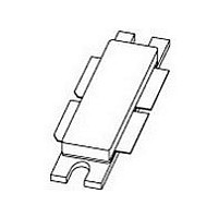
BLF6G22-180PN NXP Semiconductors, BLF6G22-180PN Datasheet

BLF6G22-180PN
Specifications of BLF6G22-180PN
Related parts for BLF6G22-180PN
BLF6G22-180PN Summary of contents
Page 1
... BLF6G22-180PN; BLF6G22LS-180PN Power LDMOS transistor Rev. 04 — 4 March 2010 1. Product profile 1.1 General description 180 W LDMOS power transistor for base station applications at frequencies from 2000 MHz to 2200 MHz. Table 1. RF performance at T Mode of operation 2-carrier W-CDMA [1] Test signal: 3GPP; test model 1; 64 DPCH; PAR = 7 0.01 % probability on CCDF per carrier; ...
Page 2
... NXP Semiconductors Compliant to Directive 2002/95/EC, regarding Restriction of Hazardous Substances (RoHS) 1.3 Applications RF power amplifiers for W-CDMA base stations and multicarrier applications in the 2000 MHz to 2200 MHz frequency range 2. Pinning information Table 2. Pin BLF6G22-180PN (SOT539A BLF6G22LS-180PN (SOT539B [1] Connected to flange. 3. Ordering information Table 3. ...
Page 3
... V drain leakage current drain cut-off current gate leakage current forward transconductance drain-source on-state resistance All information provided in this document is subject to legal disclaimers. Rev. 04 — 4 March 2010 BLF6G22(LS)-180PN Power LDMOS transistor Conditions Type = 80 °C; T BLF6G22-180PN case L(AV) BLF6G22LS-180PN Conditions Min 0 ...
Page 4
... Mode of operation: 1-carrier W-CDMA; PAR 7 0.01 % probability on CCDF; 3GPP test model PDPCH 1600 mA Symbol Parameter PAR O 7.1 Ruggedness in class-AB operation The BLF6G22-180PN and BLF6G22LS-180PN are capable of withstanding a load mismatch corresponding to VSWR = through all phases under the following conditions: V Fig 1. BLF6G22-180PN_22LS-180PN_3 Product data sheet Application information = 2112.5 MHz ...
Page 5
... G p (dB 1600 mA MHz; carrier spacing 5 MHz. Fig 4. 2-carrier W-CDMA power gain and drain efficiency as functions of average load power; typical values BLF6G22-180PN_22LS-180PN_3 Product data sheet 001aah633 50 η D (%) η 200 300 P (W) L(PEP) = 2170 MHz; 1 Fig 3. 001aah635 35 η D ...
Page 6
... NXP Semiconductors (dB 1600 mA MHz; carrier spacing 10 MHz. Fig 6. 2-carrier W-CDMA power gain and drain efficiency as functions of average load power; typical values BLF6G22-180PN_22LS-180PN_3 Product data sheet 001aah637 35 η D ACPR, (%) IMD3 30 η (dBc (W) L(AV) = 2157.5 MHz 2167 Fig 7. All information provided in this document is subject to legal disclaimers. ...
Page 7
... NXP Semiconductors 8. Test information input 50 Ω Fig 8. BLF6G22-180PN_22LS-180PN_3 Product data sheet See Table 9 for list of components. Test circuit for operation at 2110 MHz and 2170 MHz All information provided in this document is subject to legal disclaimers. Rev. 04 — 4 March 2010 BLF6G22(LS)-180PN Power LDMOS transistor ...
Page 8
... All information provided in this document is subject to legal disclaimers. Rev. 04 — 4 March 2010 BLF6G22(LS)-180PN Power LDMOS transistor C10 C11 C13 C12 OUTPUT C14 C15 C16 TB BLF6G22-180PN 001aah640 = 3.5 and thickness = 0.76 mm. r Value 10 pF 4.7 μF 220 220 μ 100 0 Ω 5.6 Ω ...
Page 9
... Note 1. millimeter dimensions are derived from the original inch dimensions. 2. recommended screw pitch dimension of 1.52 inch (38.6 mm) based on M3 screw. OUTLINE VERSION IEC SOT539A Fig 10. Package outline SOT539A BLF6G22-180PN_22LS-180PN_3 Product data sheet scale ...
Page 10
... Note 1. millimeter dimensions are derived from the original inch dimensions. Outline version IEC SOT539B Fig 11. Package outline SOT539B BLF6G22-180PN_22LS-180PN_3 Product data sheet scale ...
Page 11
... Objective data sheet 20080423 Product data sheet 20080221 Preliminary data sheet All information provided in this document is subject to legal disclaimers. Rev. 04 — 4 March 2010 BLF6G22(LS)-180PN Power LDMOS transistor Change notice Supersedes - BLF6G22-180PN_ 22LS-180PN_3 - BLF6G22-180PN_2 - BLF6G22-180PN_1 - - © NXP B.V. 2010. All rights reserved ...
Page 12
... Suitability for use — NXP Semiconductors products are not designed, authorized or warranted to be suitable for use in medical, military, aircraft, space or life support equipment, nor in applications where failure or BLF6G22-180PN_22LS-180PN_3 Product data sheet [3] Definition This document contains data from the objective specification for product development. ...
Page 13
... NXP Semiconductors’ product specifications. 13. Contact information For more information, please visit: For sales office addresses, please send an email to: BLF6G22-180PN_22LS-180PN_3 Product data sheet Quick reference data — The Quick reference data is an extract of the product data given in the Limiting values and Characteristics sections of this document, and as such is not complete, exhaustive or legally binding ...
Page 14
... Please be aware that important notices concerning this document and the product(s) described herein, have been included in section ‘Legal information’. © NXP B.V. 2010. For more information, please visit: http://www.nxp.com For sales office addresses, please send an email to: salesaddresses@nxp.com Document identifier: BLF6G22-180PN_22LS-180PN_3 All rights reserved. Date of release: 4 March 2010 ...


