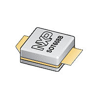
BLF6G10S-45 NXP Semiconductors, BLF6G10S-45 Datasheet - Page 3

BLF6G10S-45
Manufacturer Part Number
BLF6G10S-45
Description
RF MOSFET Power LDMOS TNS
Manufacturer
NXP Semiconductors
Datasheet
1.BLF6G10S-45112.pdf
(10 pages)
Specifications of BLF6G10S-45
Minimum Operating Temperature
- 65 C
Mounting Style
SMD/SMT
Product Type
MOSFET Power
Resistance Drain-source Rds (on)
0.2 Ohms
Transistor Polarity
N-Channel
Configuration
Single
Drain-source Breakdown Voltage
65 V
Gate-source Breakdown Voltage
13 V
Continuous Drain Current
13 A
Maximum Operating Temperature
+ 225 C
Package / Case
SOT-608-2
Channel Type
N
Channel Mode
Enhancement
Drain Source Voltage (max)
65V
Output Power (max)
1W(Typ)
Power Gain (typ)@vds
23@28VdB
Frequency (min)
920MHz
Frequency (max)
960MHz
Package Type
CDFM
Pin Count
3
Forward Transconductance (typ)
5S
Drain Source Resistance (max)
200(Typ)@6.1Vmohm
Operating Temp Range
-65C to 225C
Drain Efficiency (typ)
8%
Mounting
Surface Mount
Mode Of Operation
2-Carrier W-CDMA
Number Of Elements
1
Vswr (max)
10
Screening Level
Military
Lead Free Status / RoHS Status
Lead free / RoHS Compliant
Other names
BLF6G10S-45,112
Available stocks
Company
Part Number
Manufacturer
Quantity
Price
Company:
Part Number:
BLF6G10S-45
Manufacturer:
NXP
Quantity:
1 000
Company:
Part Number:
BLF6G10S-45
Manufacturer:
NXP
Quantity:
5 000
NXP Semiconductors
6. Characteristics
7. Application information
BLF6G10S-45_3
Product data sheet
7.1 Ruggedness in class-AB operation
Table 6.
T
Table 7.
Mode of operation: 2-carrier W-CDMA; PAR 7.5 dB at 0.01 % probability on CCDF; 3GPP test
model 1; 1-64 PDPCH; f
RF performance at V
class-AB production test circuit.
The BLF6G10S-45 is capable of withstanding a load mismatch corresponding to
VSWR = 10 : 1 through all phases under the following conditions: V
I
Symbol Parameter
V
V
V
I
I
I
g
R
Symbol
G
RL
η
ACPR
Dq
DSS
DSX
GSS
j
fs
D
(BR)DSS
GS(th)
GSq
DS(on)
p
= 25
in
= 350 mA; P
°
C per section; unless otherwise specified.
drain-source breakdown
voltage
gate-source threshold voltage
gate-source quiescent voltage V
drain leakage current
drain cut-off current
gate leakage current
forward transconductance
drain-source on-state
resistance
Parameter
power gain
input return loss
drain efficiency
adjacent channel power ratio
Characteristics
Application information
L
= 35 W (CW); f = 960 MHz.
DS
= 28 V; I
1
Rev. 03 — 20 January 2010
= 922.5 MHz; f
Dq
= 350 mA; T
2
= 927.5 MHz; f
Conditions
V
V
V
V
V
V
V
V
I
D
GS
DS
DS
GS
GS
DS
GS
DS
GS
= 2.52 A
case
= 0 V; I
= 10 V; I
= 28 V; I
= 0 V; V
= V
= 10 V
= 11 V; V
= 10 V; I
= V
Conditions
P
P
P
P
GS(th)
GS(th)
L(AV)
L(AV)
L(AV)
L(AV)
= 25
D
DS
D
D
D
= 1.0 W
= 1.0 W
= 1.0 W
= 1.0 W
= 0.5 mA
+ 3.75 V;
DS
+ 3.75 V;
°
3
C; unless otherwise specified; in a
= 72 mA
= 430 mA
= 3.6 A
= 952.5 MHz; f
= 28 V
= 0 V
BLF6G10S-45
Power LDMOS transistor
Min
21.8
5.5
7
-
Min
65
1.35
1.7
-
-
-
-
-
4
= 957.5 MHz;
DS
Typ
23
9
8
−48.5 −45.5
Typ
-
1.9
2.15
-
12.5
-
5
0.2
= 28 V;
© NXP B.V. 2010. All rights reserved.
Max
24.5
-
-
Max
-
2.35
2.7
1.4
-
140
-
-
3 of 10
Unit
dB
dB
%
dBc
Unit
V
V
V
μA
A
nA
S
Ω


