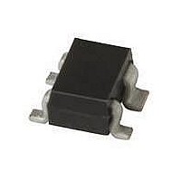
BFG540W/X T/R NXP Semiconductors, BFG540W/X T/R Datasheet - Page 2

BFG540W/X T/R
Manufacturer Part Number
BFG540W/X T/R
Description
RF Bipolar Small Signal NPN 8V 120mA 9GHZ
Manufacturer
NXP Semiconductors
Datasheet
1.BFG540WX115.pdf
(17 pages)
Specifications of BFG540W/X T/R
Dc Collector/base Gain Hfe Min
100
Mounting Style
SMD/SMT
Configuration
Single
Transistor Polarity
NPN
Maximum Operating Frequency
9000 MHz
Collector- Emitter Voltage Vceo Max
15 V
Emitter- Base Voltage Vebo
2.5 V
Continuous Collector Current
0.12 A
Power Dissipation
500 mW
Maximum Operating Temperature
+ 175 C
Package / Case
SOT-343
Other names
BFG540W/X,115
NXP Semiconductors
FEATURES
High power gain
Low noise figure
High transition frequency
Gold metallization ensures
APPLICATIONS
RF front end wideband applications in
the GHz range, such as analog and
digital cellular telephones, cordless
telephones (CT2, CT3, PCN, DECT,
etc.), radar detectors, pagers, satellite
television tuners (SATV),
MATV/CATV amplifiers and repeater
amplifiers in fibre-optic systems.
DESCRIPTION
NPN silicon planar epitaxial
transistors in 4-pin dual-emitter
SOT343N and SOT343R plastic
packages.
QUICK REFERENCE DATA
2000 May 23
V
V
I
P
h
C
f
G
|s
F
SYMBOL
C
T
FE
excellent reliability.
CBO
CES
tot
NPN 9 GHz wideband transistor
re
21
UM
|
2
collector-base voltage
collector-emitter voltage R
collector current (DC)
total power dissipation
DC current gain
feedback capacitance
transition frequency
maximum unilateral
power gain
insertion power gain
noise figure
PARAMETER
open emitter
T
I
I
I
I
I
I
C
C
C
C
C
C
s
s
BE
MARKING
PINNING
= 40 mA; V
= 0; V
= 40 mA; V
= 40 mA; V
= 40 mA; V
= 40 mA; V
85 C
BFG540W
BFG540W/X
BFG540W/XR
BFG540W (see Fig.1)
BFG540W/X (see Fig.1)
BFG540W/XR (see Fig.2)
TYPE NUMBER
= 0
PIN
opt
1
2
3
4
1
2
3
4
1
2
3
4
; I
CB
C
= 8 V; f = 1 MHz
= 10 mA; V
collector
base
emitter
emitter
collector
emitter
base
emitter
collector
emitter
base
emitter
CE
CE
CE
CE
CE
= 8 V
= 8 V; f = 1 GHz; T
= 8 V; f = 900 MHz; T
= 8 V; f = 2 GHz; T
= 8 V; f = 900 MHz; T
CONDITIONS
DESCRIPTION
2
CE
= 8 V; f = 2 GHz
CODE
N8
N9
N7
BFG540W/X; BFG540W/XR
amb
amb
amb
amb
= 25 C
= 25 C
halfpage
= 25 C
= 25 C
lfpage
100
14
MIN. TYP. MAX. UNIT
Fig.1 SOT343N.
Fig.2 SOT343R.
3
2
Top view
4
1
Top view
Product specification
120
0.5
9
16
10
15
2.1
BFG540W
MSB842
20
15
120
500
250
4
1
3
2
MBK523
V
V
mA
mW
pF
GHz
dB
dB
dB
dB


