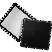
LAN88710BMR SMSC, LAN88710BMR Datasheet - Page 25

LAN88710BMR
Manufacturer Part Number
LAN88710BMR
Description
Ethernet ICs MII/RMII 10/100 Automot Transceiver
Manufacturer
SMSC
Datasheet
1.LAN88710BM_SAMPLES.pdf
(80 pages)
Specifications of LAN88710BMR
Ethernet Connection Type
10BASE-T, 100BASE-TX
Minimum Operating Temperature
- 40 C
Mounting Style
SMD/SMT
Product
Ethernet Transceivers
Standard Supported
IEEE802.3, IEEE802.3u
Supply Voltage (max)
3.6 V
Supply Voltage (min)
1.6 V
Maximum Operating Temperature
+ 105 C
Package / Case
QFN-32
Lead Free Status / RoHS Status
Lead free / RoHS Compliant
Small Footprint MII/RMII 10/100 Ethernet Transceiver for Automotive Applications
Datasheet
SMSC LAN88710AM/LAN88710BM
3.1.2.8
3.1.2.9
Receiver Errors
During a frame, unexpected code-groups are considered receive errors. Expected code groups are the
DATA set (0 through F), and the /T/R/ (ESD) symbol pair. When a receive error occurs, the RXER
signal is asserted and arbitrary data is driven onto the RXD[3:0] lines. Should an error be detected
during the time that the /J/K/ delimiter is being decoded (bad SSD error), RXER is asserted true and
the value ‘1110’ is driven onto the RXD[3:0] lines. Note that the Valid Data signal is not yet asserted
when the bad SSD error occurs.
100M Receive Data Across the MII/RMII Interface
In MII mode, the 4-bit data nibbles are sent to the MII block. These data nibbles are clocked to the
controller at a rate of 25 MHz. The controller samples the data on the rising edge of RXCLK. To ensure
that the setup and hold requirements are met, the nibbles are clocked out of the transceiver on the
falling edge of RXCLK. RXCLK is the 25 MHz output clock for the MII bus. It is recovered from the
received data to clock the RXD bus. If there is no received signal, it is derived from the system
reference clock (XTAL1/CLKIN).
When tracking the received data, RXCLK has a maximum jitter of 0.8 ns (provided that the jitter of the
input clock, XTAL1/CLKIN, is below 100 ps).
In RMII mode, the 2-bit data nibbles are sent to the RMII block. These data nibbles are clocked to the
controller at a rate of 50 MHz. The controller samples the data on the rising edge of XTAL1/CLKIN
(REF_CLK). To ensure that the setup and hold requirements are met, the nibbles are clocked out of
the transceiver on the falling edge of XTAL1/CLKIN (REF_CLK).
DATASHEET
25
Revision 1.1 (05-26-10)


