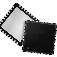
LAN88710BMR SMSC, LAN88710BMR Datasheet - Page 34

LAN88710BMR
Manufacturer Part Number
LAN88710BMR
Description
Ethernet ICs MII/RMII 10/100 Automot Transceiver
Manufacturer
SMSC
Datasheet
1.LAN88710BM_SAMPLES.pdf
(80 pages)
Specifications of LAN88710BMR
Ethernet Connection Type
10BASE-T, 100BASE-TX
Minimum Operating Temperature
- 40 C
Mounting Style
SMD/SMT
Product
Ethernet Transceivers
Standard Supported
IEEE802.3, IEEE802.3u
Supply Voltage (max)
3.6 V
Supply Voltage (min)
1.6 V
Maximum Operating Temperature
+ 105 C
Package / Case
QFN-32
Lead Free Status / RoHS Status
Lead free / RoHS Compliant
Revision 1.1 (05-26-10)
3.5
MDIO
MDIO
MDC
MDC
Preamble
Preamble
32 1's
32 1's
The Serial Management Interface is used to control the device and obtain its status. This interface
supports registers 0 through 6 as required by clause 22 of the 802.3 standard, as well as “vendor-
specific” registers 16 to 31 allowed by the specification. Non-supported registers (such as 7 to 15) will
be read as hexadecimal “FFFF”. Device registers are detailed in
on page
At the system level, SMI provides 2 signals: MDIO and MDC. The MDC signal is an aperiodic clock
provided by the Station Management Controller (SMC). MDIO is a bi-directional data SMI input/output
signal that receives serial data (commands) from the controller SMC and sends serial data (status) to
the SMC. The minimum time between edges of the MDC is 160 ns. There is no maximum time
between edges. The minimum cycle time (time between two consecutive rising or two consecutive
falling edges) is 400 ns. These modest timing requirements allow this interface to be easily driven by
the I/O port of a microcontroller.
The data on the MDIO line is latched on the rising edge of the MDC. The frame structure and timing
of the data is shown in
further described in
Serial Management Interface (SMI)
Start of
Start of
0
Frame
0
Frame
52.
1
1
Figure 3.4 MDIO Timing and Frame Structure - WRITE Cycle
Figure 3.3 MDIO Timing and Frame Structure - READ Cycle
1
0
Code
Code
OP
OP
0
1
Section 5.6.6, "SMI Timing," on page
A4 A3 A2 A1 A0 R4 R3 R2 R1 R0
A4 A3 A2 A1 A0 R4 R3 R2 R1 R0
Figure 3.3
PHY Address
PHY Address
Data To Phy
Small Footprint MII/RMII 10/100 Ethernet Transceiver for Automotive Applications
DATASHEET
and
Data To Phy
Write Cycle
Read Cycle
Figure
34
Register Address
Register Address
3.4. The timing relationships of the MDIO signals are
76.
Around
Around
Turn
Turn
Chapter 4, "Register Descriptions,"
SMSC LAN88710AM/LAN88710BM
D15
D15
D14
D14
Data From Phy
Data
Data
...
...
...
...
D1
D1
Datasheet
D0
D0


