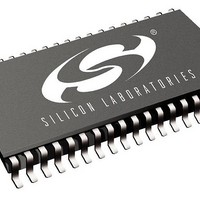
SI3210-BTR Silicon Laboratories Inc, SI3210-BTR Datasheet - Page 134

SI3210-BTR
Manufacturer Part Number
SI3210-BTR
Description
Telecom Line Management ICs Sgl Ch SLIC/Codec w/ DTMF Decoder
Manufacturer
Silicon Laboratories Inc
Datasheet
1.SI3210MPPQX-EVB.pdf
(146 pages)
Specifications of SI3210-BTR
Product
SLIC
Supply Voltage (min)
3.13 V
Supply Current
88 mA
Maximum Operating Temperature
+ 85 C
Minimum Operating Temperature
- 40 C
Mounting Style
SMD/SMT
Number Of Channels
1
Package / Case
TSSOP-38
Lead Free Status / RoHS Status
Lead free / RoHS Compliant
- Current page: 134 of 146
- Download datasheet (860Kb)
Si3210/Si3211
134
Dimension
Notes:
General
Solder Mask Design
Stencil Design
Card Assembly
1. All dimensions shown are in millimeters (mm) unless otherwise noted.
2. This Land Pattern Design is based on the IPC-7351 guidelines.
1. All metal pads are to be non-solder mask defined (NSMD). Clearance between the solder
1. A stainless steel, laser-cut and electro-polished stencil with trapezoidal walls should be used
2. The stencil thickness should be 0.125mm (5 mils).
3. The ratio of stencil aperture to land pad size should be 1:1 for all perimeter pads
4. A 3x5 array of 0.90mm square openings on 1.10mm pitch should be used for the center
1. A No-Clean, Type-3 solder paste is recommended.
2. The recommended card reflow profile is per the JEDEC/IPEC J-STD-020C specification for
C1
C2
X1
X2
Y1
Y2
mask and the metal pad is to be 60m minimum, all the way around the pad.
to assure good solder paste release.
ground pad.
Small Body Components.
E
Table 49. QFN-38 PCB Land Pattern Dimensions
Pad column spacing
Thermal pad length
Thermal pad width
Pad row spacing
Pin pad width
Pin pad width
Pad pitch
Feature
Rev. 1.5
Min.
4.70
6.70
0.20
3.20
0.80
5.20
0.50 BSC
Max.
4.80
6.80
3.30
5.30
0.30
0.90
Related parts for SI3210-BTR
Image
Part Number
Description
Manufacturer
Datasheet
Request
R
Part Number:
Description:
C°/SI3210 QFN EVALUATION BOARD WITH DISCRETE LINE INTERFACE
Manufacturer:
Silicon Laboratories Inc
Datasheet:
Part Number:
Description:
QFN 38/I°/SINGLE-CHANNEL SLIC/CODEC WITH DTMF DECODER AND BJT/INDUCTOR DC-D
Manufacturer:
Silicon Laboratories Inc
Part Number:
Description:
IC SLIC/CODEC PROGRAMMBL 38TSSOP
Manufacturer:
Silicon Laboratories Inc
Datasheet:
Part Number:
Description:
IC SLIC/CODEC PROG 38TSSOP
Manufacturer:
Silicon Laboratories Inc
Datasheet:

Part Number:
Description:
IC SLIC/CODEC PROG 38QFN
Manufacturer:
Silicon Laboratories Inc
Datasheet:
Part Number:
Description:
IC PROSLIC W/DC-DC CONV 38TSSOP
Manufacturer:
Silicon Laboratories Inc
Datasheet:
Part Number:
Description:
IC SLIC/CODEC PROG 38TSSOP
Manufacturer:
Silicon Laboratories Inc
Datasheet:

Part Number:
Description:
Telecom Line Management ICs Sgl Ch SLIC/Codec w/ DTMF Decoder
Manufacturer:
Silicon Laboratories Inc
Datasheet:
Part Number:
Description:
SLIC 1-CH 60dB 41mA 3.3V/5V 38-Pin QFN EP
Manufacturer:
Silicon Laboratories Inc
Datasheet:
Part Number:
Description:
Manufacturer:
Silicon Laboratories Inc
Datasheet:
Part Number:
Description:
Manufacturer:
Silicon Laboratories Inc
Datasheet:
Part Number:
Description:
SLIC 1-CH 60dB 41mA 3.3V/5V 38-Pin TSSOP T/R
Manufacturer:
Silicon Laboratories Inc
Datasheet:

Part Number:
Description:
SWITCH,DC-MAIN,ESTOP,32A
Manufacturer:
IMO PRECISION CONTROLS
Datasheet:

Part Number:
Description:
SWITCH,DISCONNECT,32A,DC
Manufacturer:
IMO PRECISION CONTROLS
Datasheet:
Part Number:
Description:
SMD/C°/SINGLE-ENDED OUTPUT SILICON OSCILLATOR
Manufacturer:
Silicon Laboratories Inc


