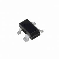
BF1100,215 NXP Semiconductors, BF1100,215 Datasheet - Page 5

BF1100,215
Manufacturer Part Number
BF1100,215
Description
MOSFET N-CH 14V 30MA SOT143
Manufacturer
NXP Semiconductors
Datasheet
1.BF1100215.pdf
(15 pages)
Specifications of BF1100,215
Package / Case
SOT-143, SOT-143B, TO-253AA
Transistor Type
N-Channel Dual Gate
Frequency
800MHz
Voltage - Rated
14V
Current Rating
30mA
Noise Figure
2dB
Current - Test
10mA
Voltage - Test
9V
Configuration
Single Dual Gate
Continuous Drain Current
0.03 A
Drain-source Breakdown Voltage
14 V
Gate-source Breakdown Voltage
13.2 V
Maximum Operating Temperature
+ 150 C
Minimum Operating Temperature
- 65 C
Mounting Style
SMD/SMT
Power Dissipation
200 mW @ Ta=50C
Transistor Polarity
N-Channel
Application
VHF/UHF
Channel Type
N
Channel Mode
Enhancement
Drain Source Voltage (max)
14V
Noise Figure (max)
2.8dB
Frequency (max)
1GHz
Package Type
SOT
Pin Count
3 +Tab
Input Capacitance (typ)@vds
2.2@9V@Gate 1/2.2@12V@Gate 1/1.6@9V@Gate 2/1.4@12V@Gate 2pF
Output Capacitance (typ)@vds
1.4@9V/1.1@12VpF
Reverse Capacitance (typ)
0.025@9V/0.025@12VpF
Operating Temp Range
-65C to 150C
Mounting
Surface Mount
Number Of Elements
2
Power Dissipation (max)
200@Ta=50CmW
Screening Level
Military
Lead Free Status / RoHS Status
Lead free / RoHS Compliant
Power - Output
-
Gain
-
Lead Free Status / Rohs Status
Lead free / RoHS Compliant
Other names
934036550215
BF1100 T/R
BF1100 T/R
BF1100 T/R
BF1100 T/R
NXP Semiconductors
DYNAMIC CHARACTERISTICS
Common source; T
C
C
C
C
F
SYMBOL
y
ig1-s
ig2-s
os
rs
Dual-gate MOS-FETs
f = 50 MHz.
T
fs
reduction
j
handbook, halfpage
= 25 C.
Fig.5
gain
(dB)
10
20
30
40
50
0
0
Gain reduction as a function of the AGC
voltage; typical values.
forward transfer admittance
input capacitance at gate 1
input capacitance at gate 2
drain-source capacitance
reverse transfer capacitance f = 1 MHz
noise figure
amb
PARAMETER
1
= 25 C; V
2
G2-S
= 4 V; I
3
V
AGC
pulsed; T
f = 1 MHz
f = 1 MHz
f = 1 MHz
f = 800 MHz; G
D
MLD157
= 10 mA; unless otherwise specified.
V
V
V
V
V
V
V
V
V
V
V
V
Rev. 02 - 13 November 2007
(V)
DS
DS
DS
DS
DS
DS
DS
DS
DS
DS
DS
DS
4
= 9 V
= 12 V
= 9 V
= 12 V
= 9 V
= 12 V
= 9 V
= 12 V
= 9 V
= 12 V
= 9 V
= 12 V
j
= 25 C
CONDITIONS
S
= G
handbook, halfpage
(1) R
(2) R
f
w
Fig.6
(dB V)
Sopt
V unw
= 50 MHz; f
120
110
100
G
G
; B
90
80
= 250 k to V
= 180 k to V
0
S
Unwanted voltage for 1% cross-modulation
as a function of gain reduction; typical
values; see Fig.27.
= B
unw
Sopt
= 60 MHz; T
10
GG
GG
= 12 V
= 9 V
24
24
MIN.
20
amb
BF1100; BF1100R
= 25 C.
28
28
2.2
2.2
1.6
1.4
1.4
1.1
25
25
2
2
TYP.
30
gain reduction (dB)
Product specification
33
33
2.6
2.6
1.8
1.5
35
35
2.8
2.8
40
MAX.
(1)
(2)
MLD158
5 of 15
50
mS
mS
pF
pF
pF
pF
pF
pF
fF
fF
dB
dB
UNIT


