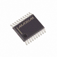
MAX9315EUP+T Maxim Integrated Products, MAX9315EUP+T Datasheet

MAX9315EUP+T
Specifications of MAX9315EUP+T
Related parts for MAX9315EUP+T
MAX9315EUP+T Summary of contents
Page 1
... 2. Functional Diagram appears at end of data sheet. ________________________________________________________________ Maxim Integrated Products For pricing, delivery, and ordering information, please contact Maxim/Dallas Direct! at 1-888-629-4642, or visit Maxim’s website at www.maxim-ic.com. Clock and Data Driver ♦ +2.375V to +3.8V Supply for Differential HSTL/LVPECL Operation ♦ -2.375V to -3.8V Supply for Differential LVECL Operation ♦ ...
Page 2
Differential LVPECL/LVECL/HSTL Clock and Data Driver ABSOLUTE MAXIMUM RATINGS ...............................................................................4. Inputs (CLK_, CLK_, SEL, EN ...........................................( CLK_ to CLK_ ....................................................................±3.0V Continuous Output Current .................................................50mA Surge Output Current........................................................100mA V Sink/Source Current ...
Page 3
Differential LVPECL/LVECL/HSTL DC ELECTRICAL CHARACTERISTICS (continued 2.375V to 3.8V, outputs loaded with 50Ω ± values are +3.3V IHD PARAMETER SYMBOL CONDITIONS ...
Page 4
Differential LVPECL/LVECL/HSTL Clock and Data Driver AC ELECTRICAL CHARACTERISTICS ( 2.375V to 3.8V, outputs loaded with 50Ω ± 80%), SEL = high or low low, V IHD V - ...
Page 5
Differential LVPECL/LVECL/HSTL (V = +3.3V 1V IHD CC with 50Ω 2V +25°C, unless otherwise noted SUPPLY CURRENT vs. TEMPERATURE 50 ALL PINS ...
Page 6
Differential LVPECL/LVECL/HSTL Clock and Data Driver PIN NAME 1 Q0 Noninverting Q0 Output. Typically terminate with 50Ω resistor Inverting Q0 Output. Typically terminate with 50Ω resistor Noninverting Q1 Output. Typically terminate ...
Page 7
Differential LVPECL/LVECL/HSTL V connected to ground, the outputs are LVPECL. The EE outputs are LVECL when V is connected to ground CC and V is connected to a negative supply. EE Input Bias Resistors When the inputs are open, ...
Page 8
Differential LVPECL/LVECL/HSTL Clock and Data Driver CLK CLK (CLK IS CONNECTED Figure 1. MAX9315 Switching Characteristics with Single-Ended Input CLK CLK Figure 2. MAX9315 Timing Diagram 8 _______________________________________________________________________________________ ...
Page 9
Differential LVPECL/LVECL/HSTL CLK CLK Q_ OUTPUTS ARE LOW Q_ EN Timing Diagram Figure 3. MAX9315 _______________________________________________________________________________________ Clock and Data Driver PLHD OUTPUTS STAY LOW 9 ...
Page 10
Differential LVPECL/LVECL/HSTL Clock and Data Driver V CC 75kΩ CLK0 CLK0 75kΩ 75kΩ 75kΩ CLK1 CLK1 75kΩ 75kΩ SEL ______________________________________________________________________________________ ...
Page 11
... Maxim cannot assume responsibility for use of any circuitry other than circuitry entirely embodied in a Maxim product. No circuit patent licenses are implied. Maxim reserves the right to change the circuitry and specifications without notice at any time. Maxim Integrated Products, 120 San Gabriel Drive, Sunnyvale, CA 94086 408-737-7600 ____________________ 11 © 2004 Maxim Integrated Products ...


