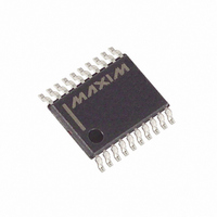
MAX9315EUP+T Maxim Integrated Products, MAX9315EUP+T Datasheet - Page 7

MAX9315EUP+T
Manufacturer Part Number
MAX9315EUP+T
Description
IC DRIVER DIFF 1:5 20-TSSOP
Manufacturer
Maxim Integrated Products
Type
Fanout Buffer (Distribution), Multiplexer , Datar
Datasheet
1.MAX9315EUP.pdf
(11 pages)
Specifications of MAX9315EUP+T
Number Of Circuits
1
Ratio - Input:output
2:5
Differential - Input:output
Yes/Yes
Input
HSTL, LVECL, LVPECL
Output
LVECL, LVPECL
Frequency - Max
1.5GHz
Voltage - Supply
2.25 V ~ 3.8 V
Operating Temperature
-40°C ~ 85°C
Mounting Type
Surface Mount
Package / Case
20-TSSOP
Frequency-max
1.5GHz
Lead Free Status / RoHS Status
Lead free / RoHS Compliant
V
outputs are LVECL when V
and V
When the inputs are open, the internal bias resistors set
the inputs to low state. The inverting inputs (CLK0 and
CLK1) are each biased with a 75kΩ pullup to V
75kΩ pulldown to V
and CLK1) are each biased with a 75kΩ pulldown to V
The maximum magnitude of the differential signal
applied to the clock input is 3.0V or V
er is less. This limit also applies to the difference
between any reference voltage input and a single-ended
input. Specifications for the high and low voltages of a
differential input (V
voltage (V
The differential clock inputs can be configured to
accept single-ended inputs. This is accomplished by
connecting the on-chip reference voltage, V
inverting or noninverting input of a differential input as a
reference. For example, the differential CLK0, CLK0
input is converted to a noninverting, single-ended input
by connecting V
ended input signal to CLK0. Similarly, an inverting con-
figuration is obtained by connecting V
connecting the single-ended input to CLK0. With a dif-
ferential input configured as single ended (using V
the single-ended input can be driven to V
with a single-ended LVPECL/LVECL signal. Note that
single-ended input must be at least V
differential input of at least 100mV to switch the outputs
to the V
Characteristics table.
If V
+2.725V to +3.8V range because one of the inputs
must be V
operation. V
becomes the high-level input when the other (single-
ended) input swings below it. Therefore, minimum V
= V
MAX9315 is V
V
supply of +2.725V. Rounding up to standard supplies
gives the single-ended operating supply range of V
V
EE
BB
EE
BB
EE
connected to ground, the outputs are LVPECL. The
= +3.0V to +3.8V.
output into V BB = V
EE
is used, the supply must be in the V
OH
+ 1.2V. The minimum V
is connected to a negative supply.
IHD
EE
and V
Single-Ended Clock Input and V
BB
- V
+ 1.2V or higher for proper input stage
CC
must be at least V
ILD
BB
Differential Clock Input Limits
OL
IHD
_______________________________________________________________________________________
- 1.525V. Substituting the minimum
) apply simultaneously.
to CLK0 and connecting the single-
levels specified in the
EE
and V
. The noninverting inputs (CLK0
EE
+ 1.2V results in a minimum
CC
ILD
1:5 Differential LVPECL/LVECL/HSTL
Input Bias Resistors
) and the differential input
is connected to ground
EE
BB
CC
+ 1.2V because it
BB
BB
output of the
- V
CC
±100mV or a
to CLK0 and
DC Electrical
EE
CC
and V
, whichev-
BB
CC
- V
, to the
and a
EE
EE
CC
BB
EE
BB
BB
or
),
=
.
-
When using the V
0.01µF ceramic capacitor to V
is not used, leave it open. The V
source or sink 0.5mA, which is sufficient to drive two
inputs. Use V
device as the V
Bypass V
ceramic 0.1µF and 0.01µF capacitors in parallel as
close to the device as possible, with the 0.01µF capaci-
tor closest to the device. Use multiple parallel vias to
minimize parasitic inductance. When using the V
erence output, bypass it with a 0.01µF ceramic capaci-
tor to V
left open).
Input and output trace characteristics affect the perfor-
mance of the MAX9315. Connect high-frequency input
and output signals with 50Ω characteristic impedance
traces. Minimize the number of vias to prevent imped-
ance discontinuities. Reduce reflections by maintaining
the 50Ω characteristic impedance through cables and
connectors. Reduce skew within a differential pair by
matching the electrical length of the traces.
Terminate outputs with 50Ω to V
equivalent Thevenin termination. When a single-ended
signal is taken from a differential output, terminate both
outputs. For example, if Q0 is used as a single-ended
output, terminate both Q0 and Q0.
TRANSISTOR COUNT: 616
PROCESS: Bipolar
Clock and Data Driver
CC
CC
(if the V
to V
BB
BB
Applications Information
EE
Controlled-Impedance Traces
only for inputs that are on the same
BB
reference.
BB
with high-frequency surface-mount
reference output, bypass it with a
reference is not used, it can be
Chip Information
Output Termination
CC
Supply Bypassing
. If the V
CC
BB
- 2V or use an
reference can
BB
reference
BB
ref-
7


